Using Serial EEPROMS
The small PICs provide a flexible programming facility but have a limited memory space to hold data. The larger PICs have more memory but have added complexity and added cost. To expand the memory space available to the PlC the 24XXXXX series of chips can be used. The 24xxxxx series range from the 24AA00 which will hold 16 bytes to the24 LC512 which will store 64k bytes into its memory. For the purpose of this article the 24LC256 will be used. The 24LC256 is a chip developed by Microchip Technology Inc and is a 32k x 8 bits (256k bits) Serial Electrically Erasable Programmable Read Only Memory (EEPROM). These little 8 pin devices, costing only a few pounds, are fantastic at storing and retrieving information and even keep their data when the power is switched off. A typical application would be the storing of data from an A-to-D converter used to good effect in John Beckers Data Logger. See Aug 99 issue). The other members of the EEPROM family have different memo 545c25f ry sizes, allow different clocking frequencies and have other attributes, but the routines used here should be equally applicable to interface these chips with any of the Microchip family of Microcontrollers.
Pins 1-3 (Address Pins) of the EEPROM allow 8 EEPROMS to be linked together on the same data line but allows each EEPROM to be individually accessed. The address pins, in normal operation, are hard wired to a logic 1 or 0 depending on the address to be taken by the chip. The clock signals are under the control of the PlC (referred to as the Master) and link to Pin 6 SCL (Serial Clock) on the EEPROM (referred to as the Slave). The master is responsible for generating the clock signals used for the data transfer. Pin 7 (WP) is the write protect pin. Hard wiring this pin to the supply will prevent any data on the EEPROM from being overwritten but 'read' will still be enabled. Any write attempt will still receive an acknowledgement from the slave that all is ok, but the write operation will not be carried out. Tying the WP pin to ground or leaving it floating will allow data to written to or read from the chip. VSS (Pin4) and VCC (Pin8) are ground and supply respectively. The EEPROM supply ranges from as low as 1.8V to an absolute maximum of 6.5V. The data is exchanged along two wires between the PlC and EEPROM. One wire passes the clock signal and the other is a two-way data line (see figure1). The data line is usually driven by an open collector output in both devices to prevent conflicts on the data line from destroying both devices. Pin RA4 on the 16F84 is an open collector terminal, ideally suited for this application. The Serial Data Line (SDA Pin 5) on the EEPROM is also open collector. A 10kΩ pull up resistor is used for the 24XX256 and is suitable for clock frequencies up to 100kHz. For 400 kHz and 1 MHz operation a 2kΩ resistor should be used.
To enable the passing of data between the two devices a serial communication protocol is used. The protocol used here was developed by Philips and is called 12C T. The protocol defines if the operation is a 'read' or 'write' and which address it operates on. Normally data is read on the leading edge of the clock pulse and the most significant bit read first. Another condition of the protocol is that data does not change while the clock pulse is high. There are two exceptions to this rule, the 'start' signal and the 'end' signal. The start of a data transmission is signalled by changing the data line from high to low while the clock is high. This is read by the slave as 'start'. The 'end 'of a data transfer is signalled by changing the data line from low to high while the clock is high. The final part of the protocol is that the receiving device, whether that is the master or the slave, will acknowledge the receipt of information. The master and slave both acknowledge the successful receipt of data by pulling the data line low. After all control or data bytes an ACK should be issued unless not required for protocol reasons. For ease of explanation the ACKs will be omitted. The master ACK is issued during the read operations while Slave ACKs are issued during read and write operations.
Now that the basics of the protocol are in place the fine detail can be filled in. After the 'start' has been sent then the next byte to be sent is a control byte (see figure 3)
Bits B7 to B4 are used to select the device. For the 24FA256 the four bits of device select are 1010. The next three bits are used to select the address of the EEPROM that is being accessed. The final bit, B0, is the read/write bit. B0 is set to 1 for a read and 0 for a write.
Following after the control byte is two address bytes. First the high address byte and then the low address byte. The control byte has told the EEPROMS which one EEPROM is being accessed, while the high and low address bytes dictate which address in that chip is being operated on. With the 256k chip there are 32k of 8 bit addresses that can be used, this covers the range 0 to 32767 (7FFF16). The top bit of the high address bit is not used by the EEPROM so only up to 7F16 can be addressed in the high byte.
We are now in a position to start transferring data. The transfer rate of data on the line, whether it is to or from the master, is under the control of the master which clocks the data on the line.
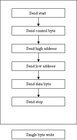
The first 'read' operation to be considered is the single byte write (figure 4). The sequence is started by the start bit. Following the start bit comes the control bit, which stipulates which EEPROM is being accessed and that a write operation is being carried out If, for example chip 6 is to be written to then the control byte will be 10101100. 1010 for device select, 1 10 for chip 6 and 0 for the write operation. If the slave has received this data correctly then it will issue an ACKnowledge by pulling the data line low. Following the control byte is the high address then the low address then the data byte and finally a 'stop' bit. This initiates the internal write cycle, which takes 5ms for byte or page. During this write time the EEPROM will not ACK signals. To prevent data being sent before the internal write cycle has been completed, the code has a delay loop at the end of the stop bit routine. This delays the master from transmitting any data or clock pulses until the slave is ready. A more efficient way of checking if the internal write cycle has finished is to use acknowledge polling. This involves sending a start bit and a control byte and detecting if an ACK is sent. If no ACK is received then the internal write is still being carried out. The start bit and control byte are repeatedly sent until an ACK is received
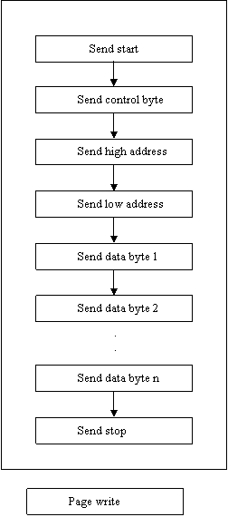
If large amounts of data had to be transferred this way then the protocol would be very slow. Fortunately the EEPROM has an on-chip page buffer, where the data is temporarily stored until the stop bit is received, and an internal address pointer. Upon initial receipt of a data byte, six low address bits are internally stored in the EEPROMs internal address pointer. The internal address pointer is incremented by one on the receipt of data. Page writes (figure 5) are limited to the size of the page within the EEPROM. The page in the 24FC256 is 64 bytes long and any attempt to cross the page boundary, regardless of the number of bytes written, will cause the address counter to roll over and overwrite data at the beginning of the page. Care, therefore, should be taken that no more than 64 bytes are sent or that a page boundary is not crossed before the 'stop' is generated. Physical page boundaries start at addresses that are integer multiples of the page buffer i.e. 0 - 3F16 and 4016 - 7F16 etc. Starting a page write at 7C16 would cross a page boundary after 4 bytes had been written. This would reset the internal address pointer to the start of the page at 4016 and carries on incrementing the internal address pointer with each new byte. The protocol for the page writes is as follows The 'start' followed by the control and the high and low address bytes then the data bytes are sent. The table write differs from the single byte write in that a 'stop' is not issued after the first byte is sent. The data bytes follow one after another until up to 64 bytes are sent and then the 'stop' is issued.
There are three types of 'read' operation; current address read, random read and sequential read.
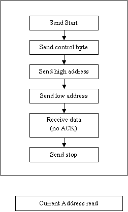
The easiest of the 'read' instructions to implement is the 'read from current address' (figure 6). This reads the data from the address set by the current settings of the internal address pointer. Thus the internal address pointer will be set to the last address +1 used and this is where the data will be read from. The start bit is sent followed by the control bit with the R/W bit set to high. Notice that after the data has been sent the master does not ACK the receipt of data but sends a stop command instead. If the master had sent an ACK the slave would have then sent the next piece of data, but more of this later.
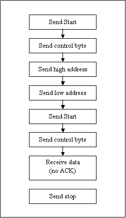
The next 'read' command, is the 'random address read' (figure 7). This routine allows the master to access any single memory location in the EEPROM. The routine starts similar to the 'single byte write'; the start bit, the command bit, and then the high and low address are sent. Then things change. The start bit is resent followed by the same control byte as before but with the R/W bit set to read. The slave then sends the read data on the data line. Again the master does not ACKnowledge the data, but sends the stop bit.
What is needed now is a routine that enables the memory of the EEPROM to be read step by step to complete the set of available operations. If the master had ACKnowledged the receipt of data in the two previous read routines the slave would have replied with the data from the next location in the EEPROM and would carry on sending data provided the master kept sending the ACK. This is the basis of the 'sequential address read' (figure 8). The internal address pointer is incremented after each read, allowing the entire memory to be serially read. Once the address reaches 7FFF16 it automatically resets to 0000 if the master sends an ACK.
The code provided does nothing more than use all these routines. The code is quite lengthy and just fits into the first bank of the 16F84. There is a table of values placed in bank1, which is used in the page write routine, which can be extensively expanded. The code looks for a 0 value, which has been placed at the end of the table. The table of values can be expanded provided that the only 0 value occurs at the end of the table and care is taken not to cross a page boundary. Users of the code should be aware that any addition of code in bank 0 would possibly cause the routine to crash. The code is provided as a basis for further experiments and was tested on TK3. The PIC frequency was resistor/capacitor driven using a 10pF capacitor and 100kΩ resistor. If when the code is run and the LEDS on PORTB display F016 then try slowing down the oscillator. If the routine runs successfully then 3A16 should be displayed.
BADDO - Writes the high and low addresses and collects the ACKs.
DDOUT - Writes out a single byte of data.
DLOOP - Writes a table of data out.
BYTIN - Reads a byte of data in.
CADRD - Read from current address.
SEQRD - Sequential read.
Memory Locations
MADDC -Address of slave.
MADDH -High memory address.
MADDL -Low memory address.
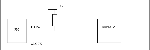
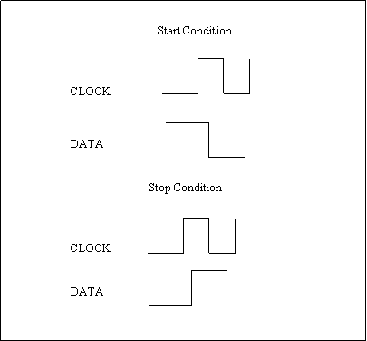
Figure 2
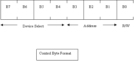
Figure 3
Random
address read
![]() Figure 6
Figure 6
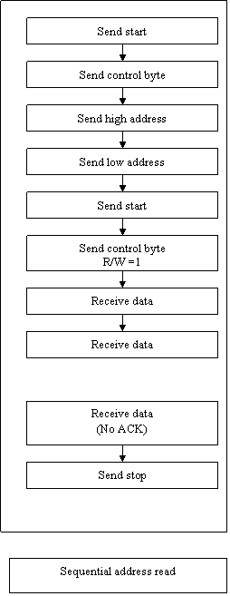
Figure 8
ROUTINE TO SEND STOP BIT
entry;- on call
exit:- clock low
Data L to H while clk H = stop
DEND: PAGE1
BCF TRISA,SDA ;Set data line to output
PAGE0
BCF PORTA,SDA ;Data Low
BSF PORTA,SCK ;Clock High
NOP
NOP
NOP
NOP
BSF PORTA,SDA ;Data High
NOP
NOP
NOP
NOP
BCF PORTA,SCK ;Clock Low
NOP
NOP
DELAY2 MOVLW H'FF ;H'40 WORKS
MOVWF COUNT1 ;This loop stops data being
LOOP2: DECFSZ COUNT1,F ;sent to slave while it is still
GOTO LOOP2 ;saving data
RETURN
READ BYTE IN
entry :- On call
exit :-RXTEMP holds read byte
BYTIN: PAGE1
BSF TRISA,SDA ;Data line set for input
BCF TRISA,SCK
PAGE0
MOVLW 8
MOVWF COUNT ;Initialise loop counter
MOVLW 0
MOVWF RXTEMP ;Clear RXTEMP ready for input
RXSTRT: RLF RXTEMP,F ;Rotate ready for next bit
BCF RXTEMP
BSF PORTA,SCK ;Clock High
BTFSC PORTA,SDA ;SDA=0 so RXTEMP=>0
BSF RXTEMP ;SDA=1 so RXTEMP=>1
BCF PORTA,SCK ;Clock Low
DECFSZ COUNT,F ;Decrement loop counter
GOTO RXSTRT
RETURN
ROUTINE TO OUTPUT BYTE
entry:- On call .W=>TXTEMP TXTEMP holds byte to be output
exit:- CLOCK low
BYOUT: MOVWF TXTEMP ;Save W in RXTEMP
MOVWF PORTB ;This left for testing purposes
PAGE1
BCF TRISA,SDA ;Data line set for output
PAGE0
MOVLW 8
MOVWF COUNT ;Count for number of bits sent
TXSTRT: BCF PORTA,SDA ;Data Low
BTFSC TXTEMP ;If Bit to be sent is low skip next instruction
BSF PORTA,SDA ;else set Data High
BSF PORTA,SCK ;Clock High
NOP ;Wait
NOP
NOP
NOP
BCF PORTA,SCK ;Clock Low
RLF TXTEMP,F ;Rotate byte to ready next bit for output
DECFSZ COUNT,F ;Decrease bits left count
GOTO TXSTRT ;Start again if COUNT is not zero
RETURN
ROUTINE TO CAPTURE ACKNOWLEDGE BIT
entry:- On Call after address or data sent
exit:- 1) EFLAG=0 if no error
2) EFLAG=2 if ACK error
ACK: PAGE1
BSF TRISA,SDA ;Data line set for input
PAGE0
BSF PORTA,SCK ;Clock High
NOP ;Wait
NOP
NOP
NOP
MOVLW H'20 ;Number of attempts to capture ACK
MOVWF COUNT ;Count to wait for ACK
LACK: MOVF PORTA,F ;Read in Data pulse
BTFSS PORTA,SDA
GOTO OUT ;ACK received
ACKERR: DECFSZ COUNT,F
GOTO LACK ;Try again to obtain ACK
BSF EFLAG ;ACK not received
OUT: BCF PORTA,SCK ;Clock low
RETURN
|