CMS 4´2 UNIT TEST & PROGRAMMING PROCEDURE
(MUX 4x2 Configuration)
CONFIGURATION OF TEST BENCH
REQUIRED HARDWARE
REQUIRED SOFTWARE
TEST PROCEDURE
EYE INSPECTION
PROGRAMMING PROCEDURE
PROCESSOR TEST (Self Test-Memory-Display-NMS ports-Outdoor Unit-Card Indication-SPI-External I/O)
DISPLAY REPRESENTATION
MUX 4X2 TEST
HITLESS SWITCH TEST
PARALLEL ALARMS TEST
MASK OF THE PULSE CHECK
SUB-MUX AND DATA INTERFACE TEST
SWITCH ALARM TEST
TROUBLESHOOTING (Under Construction)
CONFIGURATION FILES
The equipment needed for testing, are:
|
1 |
Power Supply Unit -48V/5A |
|
2 |
Multimeter (for +DC volt measure) |
|
3 |
Digital Oscilloscope which has stored the shape of the 2 Mbit/G.703/75&120 Ohm pulse |
|
4 |
Frequency meter for TTL signals |
|
5 |
BERmeter for 2 Mbit rate with 75 & 120 Ohm Interface |
|
6 |
DataCom Analyser with V.24 (RS232) interface |
|
7 |
A PC, with minimum characteristics: Pe II 350/64 MB RAM/2,5 GB HDD |
|
8 |
A serial cable for connection with the PC |
|
9 |
A JTAG programming cable |
|
10 |
An External Distribution Board with cables |
|
11 |
A 75 Ohm termination module |
|
12 |
A 120 Ohm termination module |
|
13 |
A module for external I/O test |
|
14 |
A reference rack for the tests. The structure of the rack is shown in Figure 1. |
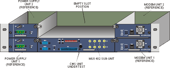
Figure . Reference rack used for the tests
The following software must be installed on the PC.
Check whether all the appropriate solder straps and jumpers are in their correct position. The solder straps and jumpers location on the PCB is shown the following figures.
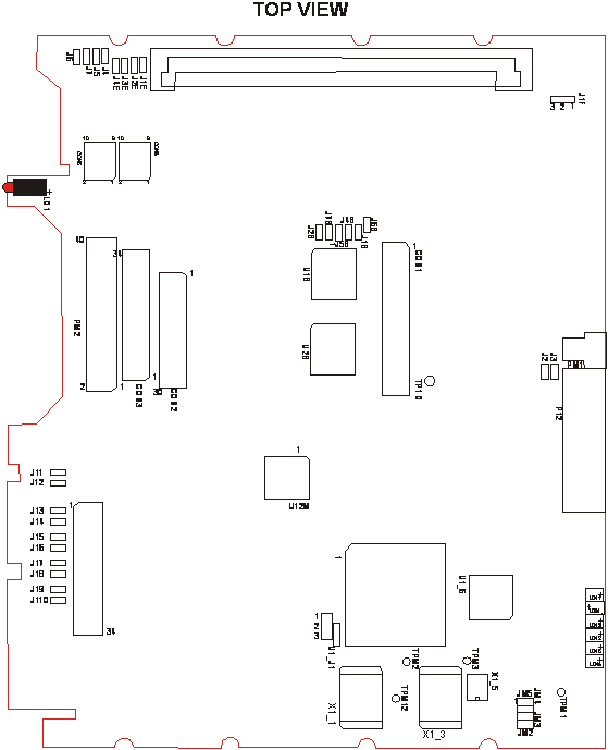
Figure
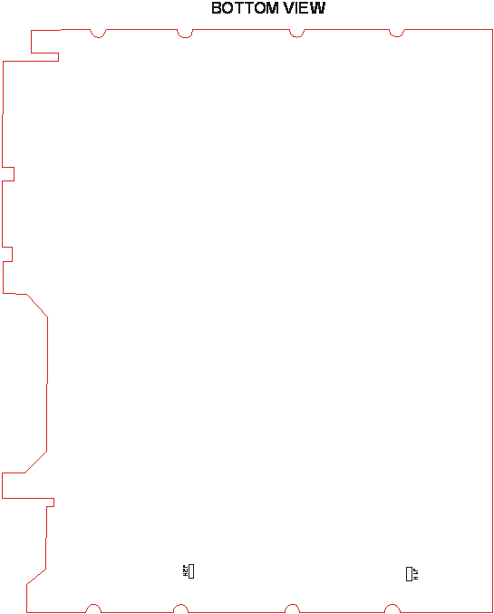
Figure
Also check whether the jumpers in Table 1 are in the correct position.
|
J1B |
OPEN 19219g620t |
J1H |
OPEN 19219g620t |
|
|
J2B |
OPEN 19219g620t |
J2H |
OPEN 19219g620t |
|
|
J4B |
OPEN 19219g620t |
JM2 |
OPEN 19219g620t |
|
|
J5B |
OPEN 19219g620t |
JM3 |
OPEN 19219g620t |
|
|
J6B |
OPEN 19219g620t |
JM4 |
OPEN 19219g620t |
|
|
J7B |
OPEN 19219g620t |
JM5 |
OPEN 19219g620t |
|
|
J2 |
OPEN 19219g620t |
U1_J1 |
POSITION 1-2 |
|
|
J3 |
OPEN 19219g620t |
JI1 |
OPEN 19219g620t |
|
|
J1F |
POSITION 1-2 |
JI2 |
OPEN 19219g620t |
|
|
J1E |
CLOSED |
JI3 |
OPEN 19219g620t (75 Ohm) CLOSE (120 Ohm) |
|
|
J2E |
OPEN 19219g620t |
JI4 |
OPEN 19219g620t (75 Ohm) CLOSE (120 Ohm) |
|
|
J3E |
OPEN 19219g620t |
JI5 |
OPEN 19219g620t (75 Ohm) CLOSE (120 Ohm) |
|
|
J4E |
OPEN 19219g620t |
JI6 |
OPEN 19219g620t (75 Ohm) CLOSE (120 Ohm) |
|
|
J4 |
OPEN 19219g620t |
JI7 |
OPEN 19219g620t (75 Ohm) CLOSE (120 Ohm) |
|
|
J5 |
OPEN 19219g620t |
JI8 |
OPEN 19219g620t (75 Ohm) CLOSE (120 Ohm) |
|
|
J6 |
OPEN 19219g620t |
JI9 |
OPEN 19219g620t (75 Ohm) CLOSE (120 Ohm) |
|
|
J7 |
OPEN 19219g620t |
JI10 |
OPEN 19219g620t (75 Ohm) CLOSE (120 Ohm) |
Table 1
For this procedure we must use the JTAG Programming Cable and the WebPack Device Programmer Software.
Perform the following steps:
|
TDO |
Pin 3 |
|
TDI |
Pin 5 |
|
TMS |
Pin 7 |
|
TCK |
Pin 9 |
|
VCC |
Pin 11 |
|
GND |
Pin 2, Pin 4, Pin 6, Pin 8, Pin 10, Pin 12, Pin 14 |
|
No Connect |
Pin 1, Pin 13 |
Table 2
IN CASE THAT THIS PROCEDURE FAILS, REFER TO TROUBLESHOOTING SECTION
The Processor TEST will check the following sections on the Central Interface Unit (CIU):
Upon Power up, the system performs a full Ram test. Bypassing the initial ram test is possible while resetting the CIU card to press the EXIT button for a few seconds. The CIU card will display RAM FAIL or RAM PASS PRESS ENTER to continue the Testing.
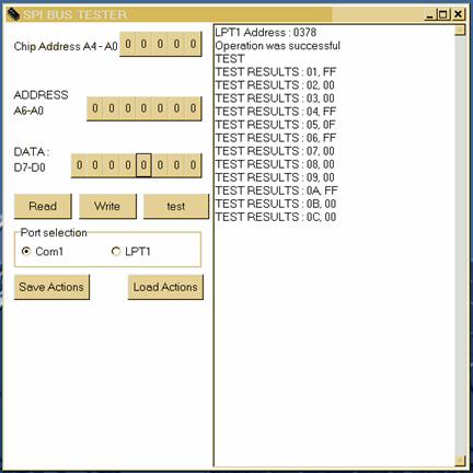
The testing is done with the use of the program "SPI BUS TESTER" shown in the Figure below, and it can me initiated in two modes, Automatic Test Mode or Manual Test Mode.
To choose which Test Mode to perform, simply select the "DATA D7-D0" section to all zeros e.g. "00000000" for Automatic Test Mode or select Manual Test Mode for individual testing (select "DATA D7-D0" e.g. 00000001 for testing the Display) and then press the button "test" for execution.
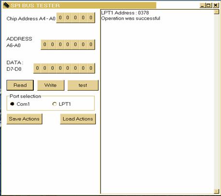
Figure
|
# |
Binary D7 - D0 |
TEST TYPE |
RESPONSE | ||
|
- |
DATA |
PASS |
FAIL | ||
|
1 |
0000 0001 |
´8 DISPLAY |
0xFF |
---- |
Visual Inspection ( Spinning "/" end-> Hello !!!) |
|
2 |
0000 0010 |
Intel Flash Memory |
0x00 |
0x01 | |
|
3 |
0000 0011 |
Atmel Flash Memory |
0x00 |
0x01 | |
|
4 |
0000 0100 |
I/O (Buzzer, CPU Led, ALM Led) |
0xFF |
--- |
Acoustic / Visual Inspection |
|
5 |
0000 0101 |
MODULE Presence |
0x00 |
0x0F |
0x0F = 0000 1 1 1 1 |
|
6 |
0000 0110 |
4 I/O EOW |
0xFF |
---- |
Visual Inspection |
|
7 |
0000 0111 |
RTC |
0x00 |
0x01 | |
|
8 |
0000 1000 |
NMS1 (serial 1) |
0x00 |
0x01 | |
|
0000 1001 |
NMS2 (serial 2) |
0x00 |
0x02 | ||
|
10 |
0000 1010 |
Buttons (Enter, Exit, Up, Down) |
0xFF |
---- |
Visual Inspection |
|
11 |
0000 1011 |
Framer (SPI) |
0x00 |
0x01 | |
|
12 |
0000 1100 |
ODU1 & ODU2 |
0x00 |
0x01 & 0x02 | |
Test Number 12 Requires A23 & B23 SORTED at the back of the backplane of the rack and also C23 & D23 respectively.
Figure
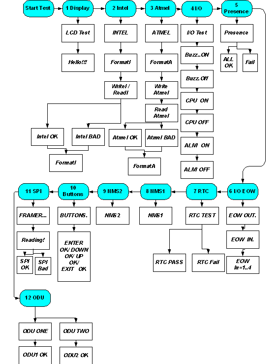
For tests 1, 6 and 10 require the Test Operator Intervention in order to complete them.
During test 1, the 1´8 LCD will spin the following characters " / - | \ " and will complete the test by displaying "HELLO!!!". For the successful completion of the test, all the pixels on the display matrix should flash ON and OFF.
For test 6, the use of the external I/O board is required. The board consists of 4 LEDs for output indication, and 4 switches for selecting input alarm activation commands. When starting the test, the 4 LEDs will turn ON and OFF one at a time, so it can test the 4 output lines. After the output test is completed, the test operator should test the 4 input lines by switching the 4 switches ON and OFF one at a time and observing the 1´8 LCD for switch indication. The test is completed successfully when all 4 LEDs turn ON and OFF and when the user switches ON and OFF the 4 switches we get a confirmation of switch activity on the display.

Figure . External I/O board
In test 10 when the respective button is held pressed (Enter, Exit, Up, Down), then on the 1´8 LCD the respective word (Enter, Exit, Up, Down) should be displayed. The test operator should verify whether the button has been pressed and then released in order to successfully complete the test.
In order for Test 6 to continue, the operator needs to PRESS ENTER
In order for Test 10 to continue, the operator needs to PRESS SIMULTANIOUS ENTER & EXIT.
When testing has finished operator MUST OPEN 19219g620t Jumper J1E.
IN CASE THAT THIS PROCEDURE FAILS, REFER TO TROUBLESHOOTING SECTION
For this procedure we must connect the serial cable, first to the serial port of the PC and then to the NMS 1 port to the CMS card on the rack. The test procedure is split into the following steps.
|
Bit Rate |
2,048 Mbit/s (Unframed) |
|
|
Line Code |
: |
HDB3 |
|
Line Impedance |
: |
75 Ohm (unbalanced) |
|
Test Pattern |
: |
PRBS-15 |
|
Tx Clock Source |
: |
Internal |
|
Rx Clock Source |
: |
Recovered from data (if required) |
|
Jitter |
: |
OFF |
|
Clock |
: |
Calibrated |
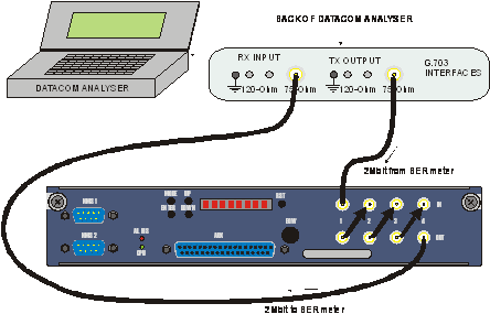
Then connect the 4X2 75-Ohm system as follows:
Figure
If the system under test is a 4X2 120-Ohm system, the connection should be as follows:
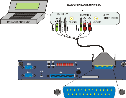
Figure .
The connections within the D25 Female connector and with the BER tester in the case of the 120-Ohm system, are shown in the following table:
|
CONNECTIONS ON THE D25 CONNECTOR AND TO THE BER TESTER |
||||||||||||||
|
BER Tester Out (+) |
BER Tester In (+) |
|||||||||||||
|
BER Tester Out (-) |
BER Tester In (-) |
|||||||||||||
|
BER Tester GND |
BER Tester GND |
|||||||||||||
The pin assignment on the D25 Male connector on the front panel of the system, is:
|
1 |
GND |
14 |
OUT-4P |
Positive OUT 4 |
||
|
2 |
OUT-4N |
Negative OUT 4 |
15 |
IN-4P |
Positive IN 4 |
|
|
3 |
IN-4N |
Negative IN 4 |
16 |
GND | ||
|
4 |
GND |
17 |
OUT-3P |
Positive OUT 3 |
||
|
5 |
OUT-3N |
Negative OUT 3 |
18 |
IN-3P |
Positive IN 3 |
|
|
6 |
IN-3N |
Negative IN 3 |
19 |
GND | ||
|
7 |
GND |
|
20 |
OUT-2P |
Positive OUT 2 |
|
|
8 |
OUT-2N |
Negative OUT 2 |
21 |
IN-2P |
Positive IN 2 |
|
|
9 |
IN-2N |
Negative IN 2 |
22 |
GND | ||
|
10 |
GND |
23 |
OUT-1P |
Positive OUT 1 |
||
|
11 |
OUT-1N |
Negative OUT 1 |
24 |
IN-1P |
Positive IN 1 |
|
|
12 |
IN-1N |
Negative IN 1 |
25 |
GND | ||
|
13 |
GND |
After all the connections as shown above have been made, the green led must remain OFF and the red leds must be switched OFF.
At the BERmeter we must see NO ERRORS.
The BER Measurement takes place for about 1 min.
IN CASE ANY OF THESE TESTS FAIL, REFER TO THE TROUBLESHOOTING SECTION
Change the Test Pattern on the BERmeter from PRBS-15 to pattern "1000". Then make the connections as shown in the following figures, depending on whether the system under test is 75-Ohm or 120-Ohm. For the connection to the Oscilloscope we must use a 75-Ohm termination module. The shape of the pulse must already be stored in the memory of the Oscilloscope, and its characteristics are shown in the figure that follows.
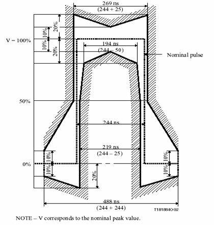
Figure
In the case of the 75-Ohm system, repeat the same procedure for all of 4 channels to verify that the mask pulse is according to G.703 specs. After finishing the test, change the test pattern back to PRBS-15.
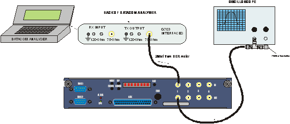
Figure
In the case of the 120-Ohm system the test cable assembly, which connects the system with the BER tester, is shown in the following figure. Tests should be repeated for all the system tributaries. Note that the way the (+) or (-) inputs of each tributary is connected to the BER tester or to the 120-Ohm termination module, is not significant.
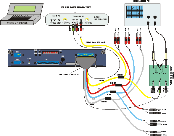
Figure .
Use the pin assignment on the D25 Male connector given earlier, in order to construct the test cable assembly, if not already constructed.
IN CASE THESE TESTS FAIL, REFER TO THE TROUBLESHOOTING SECTION
First of all we must make the following settings to the Datacom Analyser.
|
Interface: |
V.24 [DTE] [ASYNC] |
|
Tx Data Rate: |
19.2 KB/s |
|
Character Length: |
8 |
|
Stop Bits: |
1 |
|
Parity: |
None |
|
Test Pattern: |
PRBS-15 |
Before we start the procedure we must connect the serial cable, first to the serial port of the PC and then to the NMS1 port of the CMS. The test procedure is split into the following steps.
Run on the PC, the SPI Configurator Software. Select COM 1 (or COM 2) from Port Selection menu. Press the LOAD ACTIONS button, click OPEN 19219g620t and from the browser window select the C:/CIU/CMS_Mux4x2/Submux_mux4x2.txt file.
2.) Press the LOAD ACTIONS button, click OPEN 19219g620t and from the browser window select the
C:/CIU/CMS_Mux4x2/loop_framer_a_b.txt file.
3.) Then connect the External Distribution Board, first to the AUX connector of the CMS card and then the D-type connector (D9 or D25) to the Datacom Analyser. The connections are shown in the following figure.
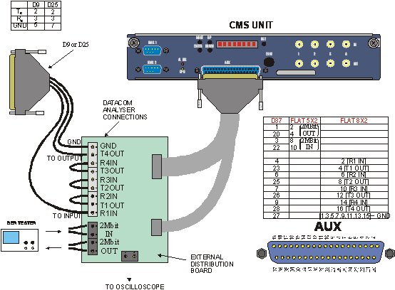
Figure .
To the Datacom Analyser we must see NO ERRORS.
The BER Measurement takes place for about 1 min.
1.) Press the LOAD ACTIONS button, click OPEN 19219g620t and from the browser window select the
C:/CIU/CMS_Mux4x2/submux_tx_path.txt file. We must read in SPI Configurator window the following value [14].
2.)Press the LOAD ACTIONS button, click OPEN 19219g620t and from the browser window select the
C:/CIU/CMS_Mux4x2/submux_rx_path.txt file. We must read in SPI Configurator window the following value [00].
3.) Press the LOAD ACTIONS button, click OPEN 19219g620t and from the browser window select the
C:/CIU/CMS_Mux4x2/submux_switch_path.txt file. When the file loads, the Datacom Analyser may have errors for a while. We reset the instrument and after that we must have the indication NO ERRORS
4.) Press the LOAD ACTIONS button, click OPEN 19219g620t and from the browser window select the
C:/CIU/CMS_Mux4x2/submux_tx_path.txt file. We must read in SPI Configurator window the following value [98].
5.) Press the LOAD ACTIONS button, click OPEN 19219g620t and from the browser window select the
C:/CIU/CMS/submux_rx_path.txt file. We must read in SPI Configurator window the following value [02].
IN CASE THAT ANY OF THIS TESTS FAILS, REFER TO TROUBLESHOOTING SECTION
According to the nature of the problem during the programming and test procedure look the below instructions.
Programming Procedure - Troubleshooting
In case that the CMS card is not programming follow the below steps (assuming that the software is already installed and we already select the appropriate file).
a. Check if the power of rack is ON.
b. Check if the JTAG cable is connected properly with the rack
c. Check if, in UB_28 pin-header there is a jumper to pin 1 with pin 2.
d. Check if the voltage in Test Point TPM1 is +2.5V +0.2V.
If all the above hardware settings are correct we must perform the following actions in the WebPack Device Programmer software.
From the pull down menus, go to OUTPUT menu and select CABLE RESET.
Then try to program again the device.
Go to the OUTPUT menu and select CABLE SETUP. Check if it is selected the parallel cable selection.
If there is still a problem then close the software and run it again.
If the there is still a problem then let the PCB out of test for further inspection.
The following text files are use for the test procedure. These files are located in C:/CIU/CMS directory.
Liu_Mux4x2.txt
Write at address : 10, 02 14
Write at address : 10, 03 04
Write at address : 11, 14 18
Write at address : 11, 15 18
Write at address : 11, 16 00
Write at address : 11, 17 00
Write at address : 12, 14 18
Write at address : 12, 15 18
Write at address : 12, 16 00
Write at address : 12, 17 00
Loop_Framer_a_b.txt
Write at address : 0A, 08 20
Write at address : 0C, 08 20
Powerdown_1_Mux4x2.txt
Write at address : 11, 14 58
Write at address : 12, 14 18
Powerdown_2_Mux4x2.txt
Write at address : 11, 14 18
Write at address : 12, 14 58
Rx_path_mux4x2.txt
Read at address : 10, 07
Switch_b_path_mux4x2.txt
Write at address : 10, 02 98
Parallel_1_Mux4x2.txt
Read at address : 10, FF
Parallel_2_Mux4x2.txt
Write at address: 0A, 24 00
Write at address: 0C, 24 00
Submux_Mux4x2.txt
Write at address: 10, 02 14
Submux_tx_path_mux4x2.txt
Read at address: 10, 02
Submux_rx_path_mux4x2.txt
Read at address: 10, 07
Submux_switch_path_Mux4x2.txt
Write at address: 10, 02 98
|