The inclusion of transistors in circuit simulation requires a model for the transistor. That is, the simulator needs to know how the transistor behaves. Specifically, the simulator requires knowledge of the terminal characteristics of the transistor. For example, for a given dc voltage VBE applied between terminals B (base) and E (emitter), what will be the current into B (IB)? The mathematical relations are obtained from theory or experimental observation. Often, the theory is very complicated, but much more simple relations serve very well as good approximations.
|
TABLE B.1 |
||
|
SPICE Name |
Math Symbol |
Description |
|
IS |
IS |
Description |
|
ISE |
ISE |
Saturation current. |
|
BF |
bF |
Base - emitter leakage saturation current. |
|
VAF |
VAF |
Ideal maximum forward current gain. |
|
BR |
bR |
Forward Early voltage. |
|
NF |
nF |
Reverse-current gain. |
|
NE |
nE |
Forward-current emission coefficient. |
The parameters for the BJT, which are to be determined in the projects as described in the following, are given in Table B.1. The parameters are obtained by fitting the mathematical expressions as used by SPICE to measured current - voltage relations.
A bipolar junction transistor is made up of a sandwich of two semiconductor pn junctions. Transistors are either npn or pnp. In the active-mode transistor state, one junction, the input junction, is forward biased, and the opposite junction, the output junction, is reverse biased. The behavior of the individual pn junction diode will first be considered to clarify forward and reverse bias.
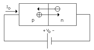
A semiconductor pn-junction diode in diagrammatic form is shown in Fig. B.1. The current and voltage of an ideal pn-junction diode are related by
Equation B.1
![]()
where VD
is the voltage applied between the p and n regions (positive at the p
terminal) 23123u201x , ID is the responding current, and ISd is the
saturation current. The thermal voltage, VT, is defined as VT
= kT/q, where T is the temperature, k is the Boltzmann constant and q is the
electron charge. At 27°C, VT ![]() 26 mV. VD is positive for forward bias and negative for
reverse bias.
26 mV. VD is positive for forward bias and negative for
reverse bias.
As illustrated by the arrows in the junction of Fig. B.1, for forward bias, the diode current consists of injection of holes from the p region (positive free carriers) into the n region and injection of electrons from the n region (negative free carriers) into the p region. The exponential factor in (B.1) is associated with the statistics of the free carriers, holes and electrons, and the effect on the lowering of the barrier to free-carrier flow of the application of the positive applied voltage.
The magnitude of ISd is dependent on semiconductor electronic properties such as doping levels and free-carrier lifetime and mobility. The magnitude of current flow for a given VD is dictated by a combination of the barrier-lowering factor (in the exponential) and the rate of free-carrier recombination; that is, carriers are annihilated by recombining with the opposite type of carrier on the opposite side of the junction from which they are injected.
A typical
value for saturation current, ISd, is 10-11 mA, such
that, for example, for VD = 0.6 V, ID ![]() 0.1 mA and increases by an order of magnitude for each additional
increment of dVD
0.1 mA and increases by an order of magnitude for each additional
increment of dVD ![]() 60 mV (at room temperature). The equation would suggest that for negative
VD and |VD| >> VT, ID = -ISd
and therefore is very small compared to the current under forward bias. In real
pn-junction diodes, the current is larger and is not independent of the value
of the reverse applied voltage. Nonetheless, it is still very small compared to
the value of current for normal forward bias.
60 mV (at room temperature). The equation would suggest that for negative
VD and |VD| >> VT, ID = -ISd
and therefore is very small compared to the current under forward bias. In real
pn-junction diodes, the current is larger and is not independent of the value
of the reverse applied voltage. Nonetheless, it is still very small compared to
the value of current for normal forward bias.
As mentioned above, the bipolar junction transistor is made up to two junctions, which share a common region. A pnp example is shown in Fig. B.2. The individual pn junctions of a transistor also exhibit diode characteristics, and the junction currents are related to the junction voltages by equations similar to (B.1). There is an essential difference that can be explained for the case of one junction being forward biased while the other junction is zero or reverse biased. Specifically, suppose that the transistor is a pnp (the other possibility being the npn) and the pn junction on the left (input junction) is forward biased and the pn junction on the right (output junction), is made to have zero bias by connecting a wire across this junction, as shown in Fig. B.2
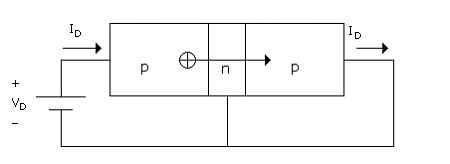
Even though the forward-biased pn junction on the left shares the n region with another pn junction (on the right), it behaves like a pn-junction diode such that the current - voltage relation for the junction still has the form of (B.1) and is
Equation B.2
![]()
The
saturation current is now designated IS, since IS ![]() ISd. [If the width of the n region is very large, the holes
injected into the n region will recombine with electrons in the n region, and
the associated current will flow entirely out through the contact to the n region.
In this limiting case, the current - voltage relation for the junction on the
left reverts to (B.1). The presence of the p region on
the right will play no role.]
ISd. [If the width of the n region is very large, the holes
injected into the n region will recombine with electrons in the n region, and
the associated current will flow entirely out through the contact to the n region.
In this limiting case, the current - voltage relation for the junction on the
left reverts to (B.1). The presence of the p region on
the right will play no role.]
In a transistor, the n-region width is made small and the statistical chance of an injected hole surviving the transit across this region, without recombining with an electron, is very high. Upon entering the p region on the right, the holes are accommodated by the exit of an equal number of holes moving out at the contact to this p region. (Actually, they are converted to electrons at the interface of the contact and semiconductor to be consistent with having only electron flow in the metal contact and device connecting metal.)
In an ideal transistor, this is the only current mechanism. The various other current components of the real transistor are discussed below. These include electron injection that would be expected from the n region into the p region of the forward-biased junction on the left (as in Fig. B.2). In practice, special fabrication techniques are employed to make this component of current very small.
In the application of a transistor in the active mode, as for example, in an analog amplifier stage, the output junction is reverse biased, as shown in Fig. B.3. The junction configuration now represents a transistor; the regions are accordingly designated as emitter (E), base (B), and collector (C). Consistent with these assignments, the current into the transistor on the left is the emitter current, IE, and the output current on the right is the collector current, IC, and according to the mechanism described above for the ideal transistor, IC = IE.
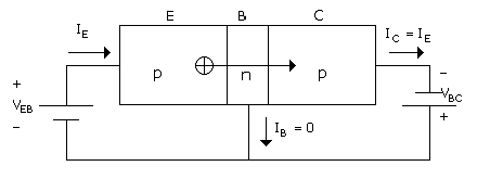
With forward bias (voltage) across the emitter - base junction and reverse bias across the collector - base junction, the emitter - base current equation, (B.2), is slightly altered, to become
Equation B.3
![]()
Variable subscripts have been changed to reflect the fact that the pnp structure is now specifically a transistor. (The parameter IS is the same in SPICE for the diode and the transistor models. ISd was used above for this discussion alone to differentiate between the two.) For reverse bias of the collector - base junction, the -1 of (B.2) is eliminated.
In this simplified version of the transistor, the output current is independent of the collector - base voltage. The possibility of infinite voltage gain is thus provided, because the output circuit behaves like a pure current source; that is, it will force current into an external resistance, which can be large without limit. This conclusion remains subject to additional alterations for the real transistor. However, in principle, the transistor mechanism as discussed is applicable short of certain limitations.
An example of obtaining gain from a transistor in an amplifier circuit is shown in Fig. B.4. A ground has been added at the n-region terminal to establish a reference. Therefore, the output voltage, VO, is defined with respect to this reference. To the transistor circuit of Fig. B.3, we have added an input signal Veb and a load resistor, RL. Note that since the input and output are referred to the base, the circuit is a common-base amplifier.
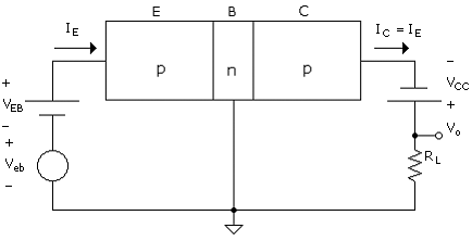
Suppose that initially, Veb = 0 and VEB is selected to give IC = 1 mA. This is, in an amplifier, the bias current. The output supply voltage is chosen to be VCC = 12 V. We select RL = 5 kW giving a bias output voltage VO = ICRL = 5 V. Note now that the collector-base bias voltage is VBC = VCC - VRL = 7V and the junction is reverse biased.
We now apply an input voltage (signal, ac, or incremental voltage) Veb = 18 mV. This increment added to VEB will cause IC to double (i.e., IC = 2 mA). The result is a new output voltage of vO(sig) = 10 V. Thus the incremental (or signal) output voltage is dVO = vO(sig) - VO = Vo = 5 V. Base - collector voltage is now vBC = VRL = 2 V and the junction remains in a reverse-bias state.
The incremental (ac or signal) ratio of output and input voltage is Vo/Vbe = 5V/18 mV = 278. Note that the gain is power-supply limited. Employment of a larger power supply permits the use of a larger RL, which results in a higher gain. We will later show that the gain is in fact VRL/VT based on an approximate linear representation between the input and output voltage. Note that in this case, the linear approximation is VRL/VT = 192, which indicates, for the example above, that the linear relation provides a fair estimate.
An alternative bias arrangement is shown in Fig. B.5. The input terminal is now that of the n region and the p terminal is a common node to the input and the output. This is the common-emitter configuration. Note that the voltage applied to the input junction has not changed, and the output junction now has a bias voltage of VEC - VEB and remains reverse biased as long as VEC>VEB.
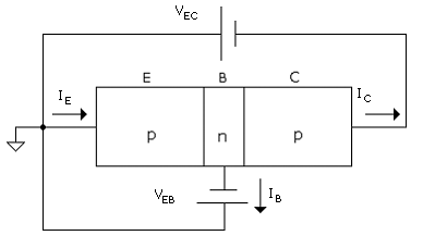
In electronic amplifiers, all three terminal configurations are possible: common base, common emitter, and common collector (emitter follower). Themost frequently employed amplifier stage is based on the common-emitter mode, but the other two serve important roles in electronic amplifiers. In all three, the emitter - base voltage is the input control-terminal voltage. In the common-emitter and common-base, the output current is the collector current and in the common collector, it is the emitter current. The common-collector configuration is usually referred to as the emitter follower.
In the subunits that follow, the detailed SPICE relations that generally relate the branch currents to the terminal voltages are developed. This includes the addition of many aspects of the real transistor which were not included in the discussion above of the highly idealized transistor.
Initially, the forward-active mode is explored, and this is followed by a discussion of the reverse-active mode. The reverse-active mode is where the situation in Fig. B.3 is reversed. Thus, VCB is positive (base - collector junction forward biased), while VEB is zero or negative. In the reverse-active mode, VCB becomes the input voltage, and the output current is the emitter current, IE.
Although the transistor is not operated in the reverse-active mode, the relationships developed for this case can be combined with those from the forward-active mode. The combination produces the general equations for relating currents and terminal voltages in transistors for all bias possibilities (i.e., where the transistor is biased out of the active mode).
In real transistors, the base width depends on the voltage applied across a pn junction. The effect is known as base-width modulation. A diagrammatic representation of the effect is illustrated in Fig. B.6. Not shown in the diagrams in Unit B.1 of the pnp structure are the depletion regions, which are shown shaded in Fig. B.6. These are the transition regions that are depleted of free carriers, and in which the barrier is formed that impedes electron and hole flow to the p regions and n region, respectively. The base width (n region) is actually the width between the depletion regions. In the diagram of Fig. B.6, we define wBo for VBC = 0 and wB for VBC > 0.
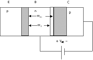
The magnitude of saturation current, IS, in (B.3) is specifically defined for VBC = 0 or wBo. In a circuit application, though, VBC will in general be nonzero and the base width can vary as shown; in the example of Fig. B.6, the base width is wB for a given applied VBC. To a reasonable approximation, the relationship between the effective saturation current with a nonzero VBC can be accounted for with the form.
Equation B.4

where ![]() is the effective saturation current
for a reverse-applied base - collector voltage. The approximate form assumes
that VBC << VAF. The expression in the denominator,
1 - VBC/VAF, comes from the fact that
is the effective saturation current
for a reverse-applied base - collector voltage. The approximate form assumes
that VBC << VAF. The expression in the denominator,
1 - VBC/VAF, comes from the fact that ![]() is approximately inversely
proportional to the base width, and the base width is roughly
is approximately inversely
proportional to the base width, and the base width is roughly
Equation B.5
![]()
The parameter VAF is called the Early voltage for forward-active operation. It has a counterpart for reverse-active operation, VAR. The base-width dependence on junction voltage is included in the nonideal factors taken up in Unit B.3
The discussion of the transistor mechanism of Unit B.1 is extended here to include base-current mechanisms, which exist in the real transistor, and the effect of base-width modulation as discussed in Unit B.2. Initially, the case of active-mode operation is discussed, and this is followed by the general-bias case, which includes the possibility of both pn junctions becoming forward biased.
In the device model for the bipolar junction transistor, the parameter bDC is
Equation B.6
![]()
where IB is the composite of all contributions to the base current. (The use of "dc" is consistent with SPICE.) This relates the output current, IC, to the input current, IB, for the transistor operated in the common-emitter terminal configuration.
In the following, the discussion is based on the npn transistor, as shown now with the schematic symbol in Fig. B.7. The npn is chosen over the pnp, as it is substantially more basic to BJTs than the pnp. This probably has to do mostly with the fact that a common-emitter stage is consistent with a positive power supply (a holdover from the vacuum-tube days), that the npn is superior in terms of frequency response, and that it has consistently been the device of BJT digital switches including the TTL. The pnp was used in the discussion above on the fundamentals of transistor action, as it is somewhat more intuitively satisfying to have the current and particle flow (where the illustration is with the hole) in the same direction.
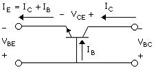
The assignment of polarities of voltages VBE and VBC is consistent with forward bias for both the emitter - base and collector - base junctions. VBC will be negative in active-mode operation. The assignment of VCE is standard, as it will be positive in active-mode operation. Current directions are assigned to correspond to the actual directions of the currents in the forward-active mode.
Base currents do not couple between junctions. Rather, as suggested in Fig. B.8, a given base current is associated with a given pn junction. In the forward-active mode, a base-current component is added to the emitter current as indicated in Fig. B.7. However, since the base - collector junction is reverse biased, the base-current contribution to the collector current is negligible and (B.3) still represents the total collector current. The collector-current relation with the base-width-modulation effect (Unit B.2) now included becomes
Equation B.7


The equation has also been generalized to include the SPICE parameter nF, the forward current emission coefficient (which is usually assumed to be 1).
The base current, for the forward-biased base - emitter junction, is made up of two terms; these are the ideal base current (because it has the same VBE dependence as IC) and the leakage base current. The leakage component is typically small enough to be neglected and often is, for simplicity, in practice.
In the absence of leakage base current, the base current is
Equation B.8
![]()
where ISBE
is the base - emitter saturation current. In the active mode, VBE is
positive, and typically, VBE ![]() 0.6V. The exponential term is, for this case, exp(VBE/nFVT)
0.6V. The exponential term is, for this case, exp(VBE/nFVT)
![]() 1010 such that the -1 is quite negligible. The -1 is necessary
for the current to go to zero for VBE = 0. This current is due to
(npn) injection and recombination of minority-carrier electrons in the base and
injection and recombination of minority-carrier holes in the emitter. Base
current could also be connected to injection of holes into the n-type emitter,
which recombine at the emitter-contact metal - semiconductor interface. In any
event, base - emitter junction base current is predominantly from injection
into the emitter, as opposed to injection into the base.
1010 such that the -1 is quite negligible. The -1 is necessary
for the current to go to zero for VBE = 0. This current is due to
(npn) injection and recombination of minority-carrier electrons in the base and
injection and recombination of minority-carrier holes in the emitter. Base
current could also be connected to injection of holes into the n-type emitter,
which recombine at the emitter-contact metal - semiconductor interface. In any
event, base - emitter junction base current is predominantly from injection
into the emitter, as opposed to injection into the base.
For this case
of no leakage current and for VBC = 0, the forward-active current gain (or current ratio) is defined as bDC ![]() bF. Using (B.6 B.7), and (B.8) (with -1 neglected), this is
bF. Using (B.6 B.7), and (B.8) (with -1 neglected), this is
Equation B.9

and ISBE = IS/bF. Consequently, the ideal base current is normally written as
Equation B.10

Note that the base current does not have VBC dependence as exhibited by the collector current. This is demonstrated to be valid in Project B
The parameter bF is the SPICE transistor-model b. Implicit in the assignment of IS (IS) and BF (bF) in the SPICE device model is the assignment of the ideal base-current saturation ISBE = IS/bF. That is, there is no ISBE (SPICE parameter) in the model. If the general active-region relation for IC, (B.7), is now used in the bDC definition, we obtain the bDC relation for nonzero VBC, namely,
Equation B.11
![]()
where bF is a constant (SPICE BF) and bDC bF for VBC = 0.
In the real transistor, there is, in general, a component of leakage current. It is associated with recombination of holes and electrons in the depletion region of the base - emitter junction. In SPICE, the leakage-current component is characterized with parameters nE (base - emitter leakage coefficient) and ISE (base - emitter leakage saturation current). When added to the ideal component, the total base current is
Equation B.12

(These are both positive into the transistor for the npn.) The parameter nE is ideally 2 (according to early, simplified theories), but in practice is typically about 1.5. When transistors are operated in or above the midrange of their rated current capacity, the leakage component becomes negligible.
For a small power transistor, the midrange starts at about 100 mA, such that the leakage term would be very significant at, for example, 1 mA. In the project on the transistor, which is designed to determine the SPICE parameters discussed here, a low-current range of less than about 1 mA is selected. The low current also avoids inadvertent rise in the temperature of the device during evaluation.
Similar equations that apply to the reverse-active mode can be obtained by direct substitution of the equivalent variables. The output current and input voltage, are, respectively, IE and VBC, while, for the reverse-active mode, VBE = 0 or negative. Based on the equivalent substitution
Equation B.13

The minus sign comes from having assigned the current direction of the emitter current out of the transistor (Fig. B.7). The parameter IS is common to (B.7) and (B.13). Equations (B.7) and (B.13) are combined to obtain the general case of VBE and VBC both positive (forward bias) in a following unit.
The reverse-operation base current is [the reverse-operation equivalent of (B.12
Equation B.14
![]()
where bR is the dc current ratio (reverse-active mode) for the case of no leakage component of base current, and is given by bR = IE/IB. In practice, the reverse ideal current gain is 0.1 < bR < 10, and therefore, the reverse-operated transistor is not a useful configuration in, for example, analog amplifiers. However, the reverse-active mode equations are essential, as is shown below, for developing the general equations for the forward mode. The general form includes the possibility that the transistor will be out of the active mode.
Although VAR (reverse Early voltage), ISC (reverse leakage saturation current) and nc (base - collector leakage emission coefficient) are officially SPICE parameters, we will not be concerned with these as they would rarely be a factor in the study of analog circuits.
The circuit shown in Fig. B.9 is used in the parameter-determination project for measuring the base current with the collector open. The collector is tied to the output channel voltage, which holds the collector - base junction in reverse bias, and therefore in the active mode. The configuration is effectively a diode (open collector) with two terminals, base and emitter, and the diode current is the base current. The base current is that of the active-mode transistor, because the collector - base junction is maintained in a reverse-bias state. Note that according to (B.12), base-current magnitude does not otherwise depend on the value of the base - collector voltage. This is shown to be valid in the project. (The base current is much different when the collector terminal is tied to ground and the base - collector junction is forward biased.)
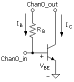
The measurement circuit includes a current sensing resistor, RB. The relation between IB and VBE for this terminal configuration is (B.12), repeated here

As noted above, the base current of (B.12) exhibits no base-collector voltage dependence other than the requirement that the transistor be in the active mode.
This is assured in this circuit since VBC is
Equation B.15
![]()
where VCC
![]() Chan0_out.
Chan0_out.
In the alternative diode circuit of Fig. B.10, the base and collector are connected such that VBC = 0 and the equation for the collector current is (B.7) with VBC = 0, or, simply,
Equation B.16
![]()
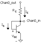
The measured current in the circuit, that is, sensed by the sensing resistor, RE, is the emitter current, IE. This is the sum of (B.12) and (B.16), which is
Equation B.17

We note that (B.12) remains valid for VBC = 0. Current measurements from the two diode circuits provide, therefore, IC, from IC = IE -IB. In the parameter measurement project, it is verified that the base current is the same for both measurement circuits. This is a means by which the independence of base current on reverse voltage is demonstrated.
In the BJT parameter determination project, parameter extraction from the exponential relations is obtained from plots of current - voltage characteristics. The form of the log of the current versus voltage provides information on the two parameters of the exponential from a straight-line curve fit. For example combining the currents from the two circuits gives, as noted, IC = IE - IB and [from (B.16
Equation B.18
![]()
The zero
voltage intercept thus reveals IS and the slope will show that nF
![]()
A simple exponential represents the base current only approximately, as it is a combination of two exponentials; that is,
Equation B.19
![]()
In the measurement of the base current, using the circuit of Fig. B.9, the measured semilog plot will appear to be a straight line. This would suggest that the current - voltage relation is a simple exponential, as in the case of the collector current. However, parameters nEprime and ISEprime vary, depending on the given narrow range of base - emitter voltage of the measurement. Note that since nF = 1 and nE > 1, nEprime will be in the range 1 < nEprime < nE.
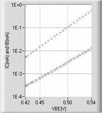
Sample measured results are shown in Fig. B.11, where the current is plotted on a log scale. For this plot, IC has been obtained from IC = IE - IB. Both plots are straight lines, indicating the exponential relationship between current and voltage for the two cases. Careful scrutiny of the lower curve (IB) should show a slight upward curvature since it is a mixture of two exponential terms, as noted. The steeper slope for emitter current is a result of the fact that nF = 1 and nEprime > 1.
The common-emitter terminal configuration can be considered the fundamental building block of BJT analog amplifier circuits. The common base and common collector are applied to some extent in more special-purpose roles, such as for high output resistance (common base) and low output resistance (common collector). Therefore, a study of the transistor in the common-emitter mode is basic to a study of analog circuits.
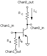
The output characteristic of the common-emitter transistor is defined as the output current (IC) as a function of the output terminal voltage (VCE) for IB (or VBE) held constant. It is very important to understand in the design of both analog and digital circuits. The output characteristic is experimentally explored in the project on parameter determination. The measurement circuit for obtaining the output characteristic is shown in Fig. B.12. This is also the circuit for measuring bDC versus IC, which is discussed below.
The equations presented in Unit B.2 are in terms of terminal voltages VBE and VBC. The common-emitter configuration has input voltage VBE but output voltage VCE. Therefore, it is preferable to eliminate VBC in the equations in favor of VCE, using VBC = VBE - VCE.
When plotting
the output characteristic, for example, from 0 < VCE < 5 V,
the range of VBC is VBE < VBC < -(5 - VBE).
Since VBE ![]() 0.5 V, VBC covers the full range from strongly forward biased
(out of the forward-active mode) to clearly reverse biased (forward-active
mode). This requires that the IC [(B.7)] and IB [(B.12)] equations be modified to include
all possibilities.
0.5 V, VBC covers the full range from strongly forward biased
(out of the forward-active mode) to clearly reverse biased (forward-active
mode). This requires that the IC [(B.7)] and IB [(B.12)] equations be modified to include
all possibilities.
To obtain an equation for IC under general biasing conditions, we start with the fundamental equation of transistor action of the BJT. This is
Equation B.20

This is a composite of (B.7) and (B.13) in which the base-modulation effects are neglected. Both of these equations are for IC and IE in the ideal transistor. (In this unit and beyond, we assume that nF = 1.) Sometimes referred to as the linking-current equation, this is symmetrical in IC and IE and neglects all components of base current and dependence of the base width on VBC and VBE.
To add an additional degree of applicability to the real transistor, base-width modulation must be added. We are interested in a relation between currents and voltages for the transistor in the forward-active mode. In this case, VBE is fixed at 0.4 < VBE < 0.6 V. On this basis, base-width modulation of the emitter - base junction can be neglected. On the other hand, the relation must apply for a VBC range, which includes relatively large negative values. Therefore, the effect of base-width modulation of the collector - base junction must be included in a modification of (B.20). If base-width modulation due to the dependence of base width on VBC is added and the substitution VBC = VBE - VCE is now made, (B.20) becomes:
Equation B.21

The general equation must include any significant base current that contributes to collector current, that is, for when the base - collector junction becomes forward biased. For this we use (B.14) with base leakage current neglected. (Leakage current is neglected throughout this unit.) This is
Equation B.22

The -1 term has been retained in order for the equation to apply at all possible polarities and values for VBC = VBE - VCE, including zero where this contribution of collector current is zero.
We note that this base current is in a loop (Fig. B.8) through the base - collector junction and is positive out of the collector terminal; IC of (B.21) is positive into the collector terminal as in Fig. B.7. Thus, the component of base current from (B.22) subtracts from the collector current to give
Equation B.23
![]()
Again, for simplicity, this equation neglects the leakage current associated with the collector - base junction [ISC term (B.14)], which is only a fair approximation for the level of IC at which we will obtain an output characteristic in the parameter extraction project on the BJT.
A plot of this equation for IC as a function of VCE can be obtained for constant VBE or constant IB. For the latter, VBE is also a variable such that the plot requires, in addition, a solution for VBE as a function of VCE for constant IB. In the project on the output characteristic, the measured data and a SPICE solution are compared during the measurement. The input circuit provides a more or less constant IB. However, the SPICE solution, which is computed by LabVIEW, is exact. It allows for a variable IB and associated variable VBE. The SPICE solution formulation used by LabVIEW is outlined below in Unit B.7. The SPICE solution is also explored in the project Mathcad file.
After measuring the output characteristic, the segment of the resulting data array from the active region (VCE > VBE) is extracted. From these data, a straight-line curve fit is obtained by LabVIEW, which produces a number for the slope. From (B.23), we obtain an equation for the active region from letting VCE > VBE, with the result
Equation B.24

The slope for the active-region equation is slope = dICact/dVCE = IC/VAF. Thus, VAF can be calculated from VAF = IC/slope, where IC is the value taken from the data array for VCE = VBE.
For the special case of VCE = VBE, one can obtain a value for IS from the relation
Equation B.25

After VAF and IS have been obtained, an iteration on bR will produce a final curve fit to the output characteristic, thereby providing a number for bR. In this manner, all three parameters of this unit are obtained: IS, bR, and VAF.
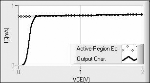
An example of a SPICE output characteristic (calculated in Mathcad), which uses the measured transistor-model parameters, is shown in Fig. B.13. Also shown is the calculated active-region plot.
The low-voltage region where IC < ICsat is called the saturation region. The voltage and current in this region are VCEsat and ICsat. In the derivation of the general equation for IC, (B.23), the leakage current of the base - collector junction was neglected. If this is not valid, the reverse bR, which is determined through curve fitting, is somewhat artificial. For example, suppose that the leakage current totally dominates the collector - base current. For this case, the general IC equation is
Equation B.26

where a new definition of a sort of bR is defined in the relation ISC = IS/bRleak. A curve fit to the measured output characteristic would give bRleak. However, because nC > 1, the result depends on the level of collector current at which the measurement is made. If, in a given measurement, the bRleak is interpreted as bR, it would function as bR in SPICE (when assigning BR to the model), but it would only be valid in a simulation for collector currents close to that of the measurement.
All components of base current are those from (B.12) (forward mode) and (B.14) (reverse mode). These are summed together to obtain the following expression for the general bias case:
Equation B.27

In the measurement circuit of the project on the output characteristic of the BJT, the circuit will provide a current source at the input and IB (to a good approximation) will be a constant. However, in the event that a precision solution for IB and VBE is required, it can be obtained by equating (B.27) to IB from the input circuit equation (Fig. B.12), which is
Equation B.28
![]()
In the Mathcad project file, a solution for VBE as a function of VCE is obtained (using a root finder) for a given VBB and RB. The result for VBE (at a given VCE) is used in (B.23) for a solution for IC, and hence the output characteristic is obtained. For this, the leakage components of base current are neglected.
In the LabVIEW output characteristic measurement project, a SPICE solution is obtained along with the measurement. The solution is obtained with LabVIEW using an iterative solution. The equations are (B.28) and (B.27) (without the leakage terms) solved for VBE. This is
Equation B.29

The iterative method consists of guessing an initial VBE and solving for IB from (B.28). This is used in (B.29), with the given VCE, to obtain a better value for VBE. The new VBE is then put back into the circuit equation, (B.28), and so on, until VBE stops changing significantly. This VBE is then used in (B.23) for a solution for IC at the specified VCE. For the complete output characteristic, the solution is repeated in increments of VCE for a range from zero up to a specified maximum. This is accomplished in LabVIEW with a Formula Node in a While Loop. The analytical formulation is explored in the project Mathcad file.
From (B.29), we note that over the full range of 0 < VCE < 5 V, for example, the limits of VBE are for VCE = 0,
Equation B.30
![]()
while for large VCE,
Equation B.31
![]()
The case of (B.30) uses bF >>
bR. For example, for bF bR = 100, the difference VBE(hi) - VBE(lo)
![]() VTln(bF bR), which is about 120 mV. In the base circuit
equation (B.28), this change would be minor
compared, for example, with a base bias voltage, VBB, of 5 to 10 V.
Thus, base current is close to a constant over the full range of VCE,
based on Chan1_out
VTln(bF bR), which is about 120 mV. In the base circuit
equation (B.28), this change would be minor
compared, for example, with a base bias voltage, VBB, of 5 to 10 V.
Thus, base current is close to a constant over the full range of VCE,
based on Chan1_out ![]() VBB = 5 V or greater, as dictated by the design goal. That
is, VBB is much greater than the change
in VBE as VCE moves from (B.30) to (B.31
VBB = 5 V or greater, as dictated by the design goal. That
is, VBB is much greater than the change
in VBE as VCE moves from (B.30) to (B.31
We note that, consistent with the limit of (B.31), the solution for IB is from
Equation B.32
![]()
Therefore, IB and VBE are constant and IC only varies with VCE due to the VCE dependence in (B.24). The value of the limit VCE is quantified in the next unit.
An equation for VCEsat (VCE in the saturation region) can be obtained using the equations for IB, (B.27) (with leakage components neglected), and IC, (B.23), to eliminate VBE. The approximate equation for IB is again

The equation for IC, (B.23), which neglects the VAF term (well justified at low voltage of the saturation region), and the -1 is
Equation B.33

Eliminating VBE between the approximate form of (B.27) and (B.33) gives
Equation B.34

where
Equation B.35
![]()
The subscript comes from "beta forced," the conventional way to define IC/IB in the saturation region. Note that by definition, bforced < bF, as IC < ICact defines the saturation region.
For example, we compute VCEsat at ICsat = IC/2. Assume that bF = 100 and bR = 1 such that bforced bF/2 = 50. For this case, VCEsat = 120 mV. Note that this is the midrange for the validity of (B.30
It should be
noted that VCEsat is not defined for bforced ![]() bF. This is because of the neglect of the -1 from
the equations. Technically, the maximum VCEsat is VCEsat
bF. This is because of the neglect of the -1 from
the equations. Technically, the maximum VCEsat is VCEsat ![]() VBE, as this is the maximum VCE at which the base
- collector junction is forward biased, the condition for the onset of the
saturation region. At VCE values very near VBE, the -1
terms in the current equations are not mathematically negligible. On practical
grounds, though, (B.34) is valid for when the output
characteristic is clearly in the saturation region.
VBE, as this is the maximum VCE at which the base
- collector junction is forward biased, the condition for the onset of the
saturation region. At VCE values very near VBE, the -1
terms in the current equations are not mathematically negligible. On practical
grounds, though, (B.34) is valid for when the output
characteristic is clearly in the saturation region.
A value for bR can be obtained, using (B.34), from one set of data points, ICsat and VCEsat from a measurement, with bF known. If this proved to vary with the ICsat chosen for the calculation, it would suggest that the discussion at the end of Unit B.5 applies. That is, the leakage current is not negligible and the effective bR bRleak, is a variable throughout the saturation region.
Since bDC/IB is a variable function of IC, the incremental bac is, in general, different from the dc bDC. (The incremental bac is often referred to as bo, but bac is consistent with SPICE.) To get an approximate value, we could calculate bac from
Equation B.42

with IC1
= IC2 and where (B.39) is used to obtain bDC at the two currents. The definition of bac is from the limiting case of IC2 ![]() IC1, that is,
IC1, that is,
Equation B.43

Performing this operation with the use of (B.39) leads to
Equation B.44

The result indicates that bac > bDC (nE > 1) and that the two converge in the limit for high IC. This is the expression used in SPICE for the incremental bac, and it is used by SPICE when NE and ISE are included in the model. Otherwise, SPICE uses bac bDC bF. (If IS and BF are not specified in the model, SPICE will use default values, typically, BF = 100 and IS = 10-16 A. For the project transistors, IS is about 10-13 A.)
|
|
Common-emitter dc current gain. |
|
|
Forward active-mode output characteristic relation. |
|
|
Forward base current. |
|
|
Reverse base current. |
|
|
Output characteristic relation. |
|
|
Collector-emitter voltage in saturation region. |
|
|
Collector-current dependence of dc common-emitter current gain. |
|
|
Collector-current dependence of incremental (ac) common-emitter current gain. |
![]()
|
Project Mathcad Files |
ExerciseB.mcd - ProjectB1.mcd - ProjectB.2.mcd - ProjectB3.mcd |
|
Laboratory Project B |
Characterization of the Bipolar Junction Transistor for Circuit Simulation |
|
PB.3 |
Diode-Connected Transistor Measurements |
|
PB.4 |
Measurement of bDC versus the Collector Current |
|
PB.5 |
BJT Output Characteristic Measurement |
|
PB.6 |
Simulation of the Output Characteristic Measurement |
|