P4.1 SPICE Parameters and Chip Diagram
P4.2 NMOS Transistor
P4.3 SPICE Equations
P4.4 NMOS Parameters from the Transfer Characteristic
P4.5 NMOS Lambda from the Transfer Characteristic
P4.6 NMOS Gamma SubVI
P4.7 NMOS Gamma
P4.8 NMOS Circuit with Body Effect
Exercises and Analysis Exercise04.mcd - Project04.mcd
|
SPICE PARAMETERS |
||
|
SPICE Name |
Math Symbol |
Description |
|
VTO |
Vtno, Vtpo |
Zero VSB threshold voltage. 24124e49y |
|
KP |
|
Transconductance parameter. |
|
GAMMA |
gn gp |
Threshold voltage parameter. |
|
LAMBDA |
ln lp |
Active-region slope parameter. |
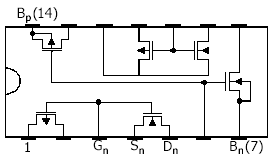
CD4007 Pin Diagram


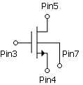
Use CD4007 pins 3 (gate), 4 (source) and 5 (drain). Connect pin 4 (source) to pin 7 (body). Connect PMOS body (pin 14) to the most positive node in the NMOS measurements, Chan0_out or ground, depending on the circuit. In the gn measurement (NMOSgamma.vi) and the transfer characteristic measurement (NMOS_Cir.vi), pin 14 is connected to ground. Note that the NMOS of pins 6, 7, and 8 has internally connected body and source. This transistor is used in a following project.
|
SPICE Equation |
Description |
|
|
|
Active region transfer characteristic and output characteristic (VDS > Veffn, VSB = 0). |
|
|
|
Active-region equation solved for VSG. |
|
|
|
Threshold voltage dependence on VSB. |
|
|
|
X variable for Vtn versus X plot in gn determination. |
![]()
|
LabVIEW Computations
Components
Procedure Set RS value. Run NMOSparsub.vi and adjust VSSinit for a minimum ID |
|
Components
LabVIEW Computations
Procedure Set RS. Run
NMOSparam.vi to obtain a set of NMOS parameters. The VI runs NMOSparsub.vi automatically with VDS = 3 V and
VDS = 10 V. The sweep stops at ID |
|
Components
Note: VGS will be larger with the body effect.
Procedure Note that PMOS body pin 14 and the NMOS drain terminal are at ground. Set RS and VSSinit from NMOSparsub.vi. Run NMOSgamsub.vi with VSB = 0 V and 3 V to verity that circuit is functioning properly. Note the change in the VGS range for the larger VSB. VSSinit is adjusted automatically for larger values of VSB, to obtain, approximately, a starting ID of about 50 mA. Default and save the Front Panel to save VSSinit. |
|
Components
LabVIEW Computations
Procedure Set RS. With NMOSgamsub.vi open, run NMOSgamma.vi to obtain Gamma. Adjust 2fF to try to match Vtno (intercept, curve fit) with Vtno (VSB = 0, transfer characteristic, graph on right). Save the results. |
|
Components Use RS from NMOSgamma.vi.
Procedure Set RS. Install SPICE parameters from NMOSparam.vi and NMOSgamma.vi. Run NMOS_Cir.vi to obtain ID versus VGS with a sweep of VSS. The iteration solution obtained in SPICEgamma.vi (Diagram below) is compared in the graph of NMOS_Cir.vi. Adjust VSSinit to obtain IDmin of about 50mA. Re-adjust Gamma for best fit. Then save a data file with your data file name. The data file must be in the folder with the Mathcad file. The file name must have a *.prn extension.
A file can be obtained from the graph of the defaulted and saved VI using XY1toDataFile.vi. The VI XY1toDataFile.vi is located in \\LabVIEW 6\User.lib\Dat_Files\Dat.llb. Note that XY1toDataFile.vi is different from XYtoDataFile2.vi, as used to obtain a data file in the Diagram of NMOS_Cir.vi. The Control Graph of XYtoDataFile2.vi accepts single plots while XY1toDataFile.vi is for graphs with two Y functions (with only one Y function in the data file). For convenience, a copy of XY1toDataFile.vi, GetDataFile.vi, is included in the Project04.llb. For clarification, XY1Y2toDataFile.vi accepts graph data with two Y functions and includes both in the data file. |
|