ECSE-2210 Microelectronics Technology
Spring 2001
Sample Quiz II (3/6/2001)
Figure below shows the structure of a Si p-i-n diode, where the i-region is intrinsic. The doping concentrations in the n- and p-regions are as marked. A voltage of magnitude |VA| is applied across the diode. Under the biased condition, the depletion layer extends in to the n and p regions as shown. Answer the following questions.
e=10-12 F/cm q=1.6X10⁻¹⁹C
![]()


(a) Determine xp, the position of the depletion layer edge on the p-side.
(b) Determine the built-in voltage of the diode in Volts.
(c) Sketch the distribution of the space charge density in Coulombs/cm3 as a function of x. Mark all the important numerical values in the graph.
(d) Sketch the electric field as a function of x. Mark all the important numerical values in the graph.
(e) What is the applied voltage, VA, across the p-i-n junction?
(f) Is the diode under forward biased or reverse biased condition?
(g) Calculate the depletion layer capacitance under the above biasing condition.
(h) The diode below is identical to the above one, except that the i-region is absent. Which one will have higher a breakdown voltage? The one above or the diode below? Explain clearly why.

a. The minority carrier concentration in a p-n junction under a biased condition is shown below. The total number of excess minority carriers in the n and p regions (i.e. the shaded regions) are marked in the figure. Assume that the area of the diode is 1 cm2 and tn =2ms on p-side and tp = 1ms on n-side. Calculate the total current passing through the diode.
![]()
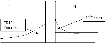
b. A particular ideal p+-n junction has reverse saturation current of 2X10-14Amp. The hole lifetime in the n-side is 2ms. What will be the diffusion capacitance of the diode if the diode is forward biased to 0.6V? What is the physical origin of this diffusion capacitance?
c. A planar Si p+-n step junction diode has n-side doping of 1015 cm-3. Suppose the reverse breakdown of this diode happens when the peak electric field, ECR reaches 2 X 10⁵ V/cm, calculate the breakdown voltage of the diode.
d. Shown below is the electric field profile in the depletion region of semiconductor pn junction at thermal equilibrium. If the doping on the p-side is 1015cm-3, what will be the doping on n-side?

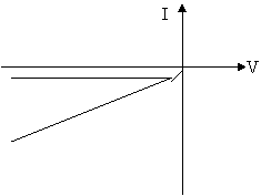
e. The reverse bias characteristics of an ideal and real diodes are shown below. Explain clearly the source of higher reverse current for a real diode. Why does the reverse current increase for the real diode as the magnitude of the reverse voltage is increased?
Problem 3
A silicon npn transistor has the following parameters. The transistor is biased with VBE = 0.6V and the C-B junction is reverse biased. Answer the following.
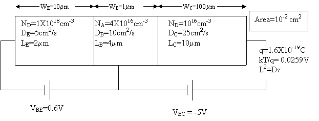
a. Minority carrier concentration profiles in the base, emitter and collector under the above biasing conditions are shown below. Calculate the numerical values of concentrations marked in the graph.

b. Calculate the collector current Ic under the above biasing conditions. Ignore the effect of base-width-modulation for this calculation.
c. Calculate the base current Ib.
d. Calculate the base transport factor, aT.
e. Calculate the emitter injection efficiency g.
f. Calculate the common emitter current gain, bdc.
g. Calculate an approximate value of punch-through voltage across C-B junction.
h. Suppose the base width is reduced to 0.5um, what will happen to bdc under the above biasing conditions? (Increase or decrease: choose one). Recalculate the new value of bdc.
The transistor is biased such that the minority carrier concentration in the base is as follows:
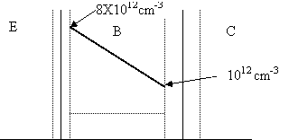
i. The transistor now is in (forward active, reverse active, cut-off, saturation: choose one) mode. Justify your answer.
j. Calculate the voltage applied across B-E junction (VBE) and B-C junction (VBC).
k. Calculate the recombination part of the base current, IBR.
a. The npn switching transistor used in the circuit below has the following parameters:
Minority carrier lifetime in base, tB = 100 nS; bdc = 100. Assume g=1. If RB is 25kohm, how long will it take for the collector current to reach steady state value after the switch is closed?
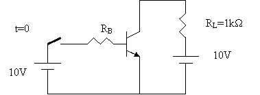
b. Suppose RB is decreased to 10Kohm. The turn-on time will (increase, decrease, remains the same: choose one). The turn-off time will (Increase, decrease, remains the same: choose one) Justify your answer.
c. Two pnp BJTs are identical except that the collector and base dopings are interchanged as shown below. Which transistor will exhibit the greater sensitivity to base width modulation under active mode biasing? Explain.
BJT A BJT B
![]()
d. Among the two BJTs above, which one will have higher bdc? Explain.
|