High-gain stages in amplifiers are usually some form of differential stage or common-source stage. These are inherently high-output-resistance stages and are not suitable for low-impedance loads. The solution for a requirement to drive low-impedance loads is to insert a buffer stage between the output of the common-source 939b112j stage and the load. The buffer will be a source-follower stage. The name follower comes from the fact that to a good approximation, the output voltage follows the input voltage; that is, it has an open-circuit gain of unity and low output resistance.
Although the output voltage/input voltage relation is sometimes loosely referred to as the gain, it would be more accurate to label it the voltage transfer function, as the "gain" is less than 1. The transfer function is explored in the following for various possibilities of degrees of approximation in the linear circuit.
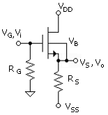
The circuit diagram shown in Fig. 7.1 uses for the transistor a symbol that includes the body connection. This is to emphasize the fact that the output (source) of the source follower is generally (and usually) at different dc and signal potentials from the body. In Project 8 we measure the gain for both the connection shown (which we can make for this special case of one transistor on the chip being used) and with the body connected to VSS, which is signal ground. The latter demonstrates the extent of the influence that the body effect has on the gain when it is not possible to connect the body and source together as shown in Fig. 7.1

The design of the stage will often consist of setting the dc output at VO = 0 V (for a dual power supply), as this will be the final (output) stage. Therefore, RS will be selected based on the design drain current from RS = |VSS|/ID. It is then necessary to determine VGS in order to determine the VG = VGS required (which will be set by the dc circuitry of the preceding circuit).
For the usual practical application, body voltage, VB = VSS. With VS = 0 V, VSB = |VSS|. Thus, the threshold voltage, including body effect, will be
Equation 7.1
![]()
and the gate bias voltage will be obtainable from
Equation 7.2
![]()
If the source and body are connected, as in Fig. 7.1, Vtn is replaced with Vtno.
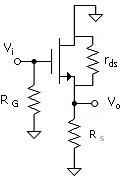
A signal circuit is shown in Fig. 7.2, where the dc supplies have been replaced with ground. Also, the internal resistance, rds = 1/gds, of the transistor has been included in the signal circuit. Note that it is in parallel with RS since the drain is tied to signal ground. Assume for now that source and body are connected as in Fig. 7.1

Regardless of the terminal configuration, for infinite output resistance and with the body and source connected, the relationship between the drain current and gate - source control voltage of the transistor is ( ) with gds = gmb = 0, which is [(
![]()
In the source-follower circuit, the output resistance of the transistor can be included in the source-follower load and ( ) effectively applies.
The transconductance for the circuit configuration with a source resistor was shown in Unit 4 to be [(
![]()
where,
for this case, ![]() is the source-follower load, which
includes the transistor output resistance and is
is the source-follower load, which
includes the transistor output resistance and is
Equation 7.3
![]()
Then using
Equation 7.4
![]()
the "gain" (the transfer function is less than unity) is determined to be
Equation 7.5
![]()
Ideally, this
is a unity gain, as would be the case for ![]() . In bipolar transistors, this
condition is closely approached. However, in MOSFET source followers, the ideal
case is in general not reached. As we will see below, this deficiency is
enhanced when the body effect is included.
. In bipolar transistors, this
condition is closely approached. However, in MOSFET source followers, the ideal
case is in general not reached. As we will see below, this deficiency is
enhanced when the body effect is included.
Note that av is
Equation 7.6

This is the
expression for a simple voltage divider. Thus the source follower is the
equivalent of a unity-gain circuit with load ![]() and output resistance 1/gm.
We can conclude that the transistor viewed from the source has an output
resistance of 1/gm.
and output resistance 1/gm.
We can conclude that the transistor viewed from the source has an output
resistance of 1/gm.
Finally, with
![]() separated into its component parts,
the source-follower gain becomes
separated into its component parts,
the source-follower gain becomes
Equation 7.7

In general, the gds parameter can be dropped. The ratio of gm/gds is
Equation 7.8
![]()
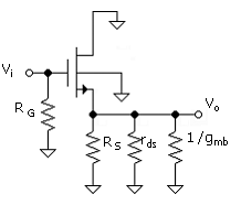
Suppose now, as in Fig. 7.3, that the body terminal is connected to VSS, which is signal ground. Following the definition of the body-effect transconductance, gmb, the component of Id due to source-body voltage Vsb is [from (
Equation 7.9
![]()
Since the body is at zero potential (signal), this is
Equation 7.10
![]()
This component of current can be included in the circuit, as shown in Fig. 7.3, with an additional resistance in parallel with RS of value 1/gmb. That is, the body-effect contribution to the drain current is a voltage-dependent current source, where the voltage is the same as that across the current source.

With the body-effect addition, the source-follower gain expression is modified to the following:
Equation 7.11

The body-effect parameter is related to gm by [(
gmb = hgm
with
![]()
With the substitution of ( ) in ( ), the gain is
Equation 7.12

In modern integrated circuits, resistor RS will be replaced with a current-source output resistance, which is significantly greater than RS. The source-follower gain is, in this case, approximately (with no external load)
Equation 7.13
![]()
Parameter h will typically be in the range 0.1 < h < 0.2.
Note that the body effect degrades the "gain" significantly below the ideal unity. In the project on the source-follower circuit, we measure the voltage transfer function of the source follower for a range of dc drain current with body and source connected and with the body connected to VSS. The resulting curves will be compared to demonstrate the body effect on the transfer function. A curve fit of the SPICE equation to measured data will provide for an alternative determination of parameter gn. This value should be close to the value obtained from dc measurements.
7.4 Summary of Equations
|
|
Project Mathcad Files |
Exercise08.mcd - Project08.mcd |
|
Laboratory Project 8 |
NMOS Source-Follower Stage |
|
P8.2 |
Source-Follower DC Evaluation |
|
P8.3 |
Source-Follower Voltage Transfer Relation |
|
P8.4 |
Source-Follower Voltage Transfer Relation with Body Effect |
|