Table of Contents
Table of Contents i
List of Figures ii
List of Tables ii
Executive Summary 1
1.0 Background 2
2.0 Problem Definition 3
3.0 Design Selection 4
3.1 Designs Considered 4
3.2 Design Solution 4
3.3 Analog Circuits Tested 5
3.3.1 FM Transmitters with Tunnel Diode 5
3.3.2 FM Transmitters without Tunnel Diode 6
3.4 Detailed Description and Justification of Design Chosen 6
4.0 Fabrication and Testing 7
4.1 Prototype Testing and Performance 7
4.2 Printed Circuit Board 9
4.2.1 Components 10
4.2.2 Layout 10
4.2.3 Testing 11
4.2.4 Performance 12
5.0 Results and Conclusions 13
5.1 Final Evaluations 13
5.2 Future Modifications 14
6.0 Expenses 15
7.0 Acknowledgements 16
References 17
Appendix A - Design #1 Functionality 20
A.1 CODEC 20
A.2 Microcontroller 20
A.3 Digital RF Transceiver 21
A.4 Design Evaluation 22
Appendix B - Design #2 Functionality 23
B.1 Transceiver Module 23
B.2 Microcontroller 24
B.3 Design Evaluation 24
Appendix C - Additional Analog FM Transmitters 25
Appendix D -
Surface
List of Figures
Figure 1. Transmission stage from previous design 3
Figure 2. FM transmitter chosen for final design 7
Figure 3. FM transmitter prototype circuit 8
Figure 4. Output signal from prototype circuit 9
Figure 5a. Top view of PCB 10
Figure 5b. Bottom view of PCB 10
Figure 6a. Layout of the top of the PCB 11
Figure 6b. Layout of the bottom of the PCB 11
Figure 7. Output waveform from PCB transmitter 12
Figure 8. Final FM transmitter within earmold 13
List of Tables
Table 1. Transmitted Distances of Prototype With and Without an Antenna 8
Table 2. Expenses 15
EXECUTIVE SUMMARY
EarTalk is a communication system developed by the National Institute for Occupational Safety and Health (NIOSH) that consists of a microphone embedded in an earplug. The microphone senses the user's voice via bone conduction through the head and creates an electrical representation of the user's speech. This electrical signal passes by wire to external circuitry that restores the natural speech quality lost during bone conduction. NIOSH requested a wireless transmission system to eliminate the wires connecting the earplugs to the external circuitry. This report presents a functional design solution for the wireless transmitter.
The implemented design is an analog FM transmitter built from basic circuit components. The transmitter operates in the 88-108MHz radio band. It meets the criteria of a transmission distance of 5-10 inches, a supply voltage of less than 1.4 Volts, and a size small enough to fit within the ear.
Once the team selected a design, a prototype transmitter was constructed on a breadboard from common thru-hole components. This initial prototype yielded excellent results and transmitted a voice signal clearly in excess of the required 5-10 inches.
In order to miniaturize the transmitter, the next step was to design and construct a printed circuit board (PCB). The size of the circuit was greatly reduced by developing a double-sided PCB that was small enough to fit directly within the ear. While the PCB transmitter did not function as well as the prototype, it did produce promising results. Unlike the prototype, the PCB circuit required an antenna to transmit the signal effectively.
Future work on the wireless transmitter could include the design of a small antenna. In addition, minor modifications to the PCB design might produce better transmission results.
BACKGROUND
In environments with high levels of background noise such as in tanks, on aircraft carrier flight decks, or in firefighting situations, communication by a conventional microphone and speaker headset is not possible. Hearing protection in the form of earplugs and/or earmuffs is often required. Not only is hearing protection important, but a clear form of communication is also vital in situations such as firefighting where it can mean the difference between life and death (Kardous, 2003, p. 44).
In order to provide a clear channel of communication, NIOSH has developed a system called EarTalk that consists of a microphone embedded in an earplug. When placed within the ear, the microphone in the earplug senses the acoustic vibrations produced by the wearer's voice that were transmitted through acoustic coupling via bones in the head. As a person speaks, acoustic vibrations in the head cause the eardrum to vibrate, and this vibration excites air in the ear canal (Kardous, 2003, p. 43). The microphone in the earplug senses the acoustic signal and transduces it to an electrical signal. This electrical signal passes by wire to a circuit that amplifies and conditions the signal. This circuitry restores the natural voice quality that is lost as the acoustic signal passes through the user's head via bone conduction. The restored electrical signal is transmitted wirelessly using radio frequency (RF) transmission to those receiving the communication (Franks, et al., 1995, p. 4).
Previously, the EarTalk design used wires to pass the
electrical signal from the earplug to the amplifying and conditioning
circuitry. Wireless transmission of the
signal would improve the mobility of the user and the EarTalk system. Two teams of three electrical engineering
students were given the task of developing this wireless transmission system as
part of Capstone Design at the

Figure . Transmission stage from previous design.
Unfortunately, the team was unable to implement their design because of time constraints. However, their research and simulations provided a good reference for future work and eventual implementation of the wireless transmission system.
The second team created an analog transmission system to pass the signal from the ear to the external circuitry. This system consisted of a two-stage, off-the-shelf amplifier and an analog RF transmitter (Griffin, et al., 2003, p. 2). While this system functioned correctly, the circuit could not be contained in or around the ear. The analog transmitter required a surface area of approximately 3 square inches. Therefore, this system would not fit within or immediately outside the ear to allow the user to wear earmuffs for further hearing protection.
PROBLEM DEFINITION
The National Institute for Occupational Safety and
Health (NIOSH), a division of the Center for Disease Control (CDC) in
DESIGN SELECTION
3.1 DESIGNS CONSIDERED
The first conceptual design was a digital transmission system. When implementing a digital wireless transmission system, four components are necessary: a microphone, amplifier, ADC, microcontroller, and a digital RF transceiver. This design consisted of integrating discrete components. Appendix A contains a detailed description of this design as well as a detailed description of each component.
The second design involved a highly-integrated, digital RF transceiver module in conjunction with a microphone and a microcontroller. Appendix B contains a detailed description of this design as well as a detailed description of each component.
3.2 ANALOG DESIGNS
Based on the criteria laid out by the team and the specifications set by NIOSH, an analog FM transmitter was selected to miniaturize the current EarTalk system. Of the three options considered, the analog FM transmitter was the smallest and fit within the ear. In addition, this design required no antenna because the transmission distance was so small. The circuit was easy to build and implement since only basic circuit components were required. Several analog designs require 1.5 Volts or less for operation, meaning that the low-power criterion was easily satisfied. Overall, this design was the most feasible based on the knowledge and experience of the team, the time constraints of the project, and specifications set forth by NIOSH.
An additional advantage of the analog FM transmitter was the simplicity of the design. Therefore, it was relatively easy to implement compared with the two previous designs. In addition, careful circuit layout produced an analog transmitter small enough to fit within the ear. Fabrication of a printed circuit board (PCB) for our specific design resulted in a transmitter much smaller than either of the digital designs. A second advantage of this design was that a simple FM pocket radio could receive the transmitted voice signal. The two digital designs required the development and construction of a receiving stage because they operated at frequencies much higher than the conventional FM radio range. The final advantages of the analog transmitter were the low cost and small size. In addition, the cost was significantly lower than the other designs due to the basic components required.
3.3 ANALOG CIRCUITS TESTED
After researching existing analog FM transmitter designs, it was discovered that there were basically two types of active components used to modulate the carrier signal. Tunnel diodes and transistors were used in combination or alone to generate the oscillation necessary for FM transmission. The theory of operation behind designs that contain tunnel diodes and those that did not is different due to the physical characteristics of the devices; however, the largest discrepancy between these two types of transmitters was their performance.
FM Transmitters with Tunnel Diode
Tunnel diodes operate in both positive and negative resistance modes based on the voltage applied across the diode. This unique characteristic curve causes the diode to become an oscillator as the voltage is varied. Appendix C contains two schematics of the tunnel diode circuits that the team put a significant amount of effort into testing. The team was initially very excited about these tunnel diode FM transmitters because of their minimal number of components. However, it was discovered that there were few resources available regarding the operation and troubleshooting of tunnel diodes. The tunnel diodes themselves were very expensive components, approximately $30 each, so the implementation of each circuit was also very costly. There are very few companies that still fabricate tunnel diodes, and it was very difficult to interface with these companies. Although the tunnel diode designs initially seemed like they would be an excellent solution, the performance of these circuits was very poor. The lack of functionality and availability of the necessary components made tunnel diode FM transmitters an unrealistic choice.
3.3.2 FM Transmitters without Tunnel Diode
Although transistors have very different characteristics than tunnel diodes, they can still be used in a similar way to produce FM transmission. Transistors, when supplied with varying inputs, will oscillate and amplify the oscillation. In general, the FM transmitter circuits considered that contained only transistors as the active devices had more components than the tunnel diode circuits and required higher operating voltages. However, there were a few designs that met the necessary specifications. Appendix C contains one of the FM transmitters tested that used only transistors for modulation. Although this circuit had poor performance, it was much easier to work with given the availability and simplicity of the components. It became clear that a transmitter requiring no tunnel diodes would be a better option as a long as it met specifications and clearly transmitted voice on FM frequencies.
3.4 DETAILED DESCRIPTION AND JUSTIFICATION OF DESIGN
After several rounds of initial testing, the team decided to select an FM transmitter design that did not contain a tunnel diode. Figure 2 shows the circuit chosen for the final design.
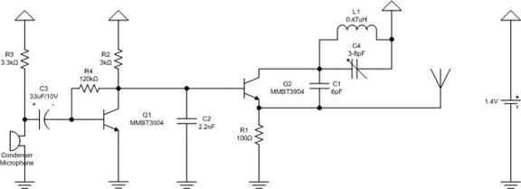
Figure 2. FM transmitter chosen for final design
The transmitter chosen to undergo miniaturization and final implementation has a 1.4V supply voltage that can be provided by a size 10 hearing aid battery. Preliminary calculations (shown in Appendix C) indicated that this transmitter could operate for more than 40 hours on a single battery. The circuit contains 11 components including two transistors and no tunnel diode. It is composed of basic resistors, capacitors, transistors, and an inductor. These components are inexpensive and readily available in both regular and miniature form. They are also relatively simple to implement and manipulate. This design was selected for implementation because it performed the best during the initial testing phase. This circuit also met or exceeded all of the required specifications. It showed exceptional promise for implementation in the final package.
FABRICATION AND TESTING
4.1 PROTOTYPE TESTING AND PERFORMANCE
The first step toward building a functional design was to construct a circuit prototype on a breadboard out of standard off-the-shelf components. It was extremely important for the team to have a working model of the circuit that could easily be manipulated to reach optimization. Figure 3 illustrates the constructed circuit prototype.
Antenna

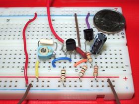
Figure 3. FM transmitter prototype circuit.
Figure 3 also shows an antenna wire that is connected across the 6pF capacitor. Through testing the circuit with various antenna lengths and materials, it was found that including an antenna reduced the performance and transmission distance of the circuit. Since the circuit contained several active components and wires, it produced enough radiation for a handheld FM radio to receive a clear signal without an antenna. Thus, the antenna was eliminated from the design which also reduced the complexity and price. The following table displays the estimated distance the circuit transmits with and without the antenna:
Table 1. Transmitted Distances of Prototype With and Without an Antenna.
|
DISTANCE (ft.) |
|
|
With Antenna | |
|
Without Antenna |
One of the key features of this circuit is that the variable capacitor can be adjusted to change the transmission frequency. The estimated oscillation frequency of the prototype tank circuit was approximately 104 MHz. The corresponding values of the variable capacitor and inductor needed to produce this carrier frequency are 5pF and 0.47uH, respectively. Figure 4 shows the transmitted signal of the circuit. The carrier signal and frequency modulation can both be seen.
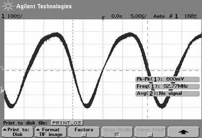
Figure 4. Output signal from prototype circuit.
After successfully creating the circuit shown in Figure 3, the team connected the transmitter to a 1.5 Volt battery power supply via a battery holder. The battery holder contained six inch leads that connected it to the circuit. The circuit transmitted a more distorted signal than the one that was received using the DC power supply. Extending the leads of the battery reduced the amount of noise the radio received.
PRINTED CIRCUIT BOARD
Size was a crucial factor in the design because the circuit needed to fit within the ear to allow for the use of hearing protection to be worn over the ears. Miniaturization of the transmitter system required implementing the circuit on a printed circuit board. Figure 5a and 5b show the top and bottom view, respectively, of the transmitter PCB.
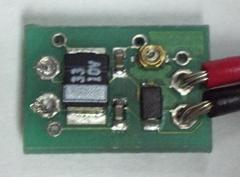
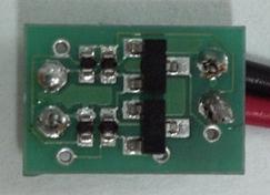
Figure 5a. Top view of PCB. Figure 5b. Bottom view of PCB.
4.2.1 Components
The two component mounting options considered for the PCB were thru-hole and surface mount. Surface mount components were the best choice for this circuit due to the large number of parts that could be placed on the board in a minimal area. A complete list and description of each part used can be found in Appendix D.
An antenna was not included in the PCB design for two primary reasons. Excellent results were obtained from the transmitter prototype without an antenna, and an antenna would significantly increase the size and complexity of the entire system. However, testing of the PCB illustrated the need for an antenna, as explained in Section 4.2.4.
4.2.2 Layout
The layout for the PCB was designed using the Eagle layout software. In order to fully miniaturize the circuit, parts were placed on both the top and bottom of the board. The double-sided board essentially cut the size of the board in half compared to a single-sided board.
Several board layouts were created in order to compare sizes and ease of routing wire traces. The final layout was selected based on the overall board size, length of wire traces and number of vias, relative location of parts, and accessibility of the variable capacitor for adjustment. Figures 6a and 6b, shown below, depict the final top and bottom layouts of the board in Eagle, respectively.
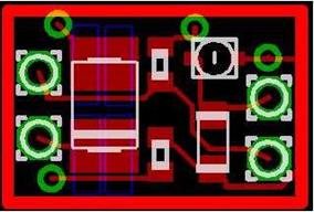
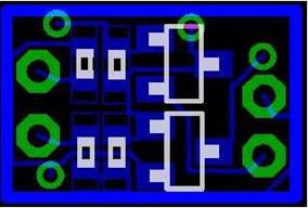
Figure 6a. Layout of the top of the PCB. Figure 6b. Layout of the bottom of the PCB.
Figure 6b shows the placement of the four resistors and two transistors on the bottom of the board. In order to place these components on the bottom, new libraries had to be created to change the associated layers from the top to the bottom.
4.2.3 Testing
Initial testing of the PCBs consisted of applying a DC voltage of 1.4V to the circuit and then probing internal nodes to display the output on an oscilloscope. By observing the voltages at various nodes in the circuit, the team found that the initial PCBs did not produce an oscillating carrier signal. Instead, it was found that there were pure DC voltages throughout the circuit. These voltage measurements indicated that there was a problem with the circuit components, layout, or construction.
Further testing included measuring the values of the various components with a digital multi-meter (DMM) or RLC meter. The values were then compared with the board layout in Eagle to verify that each component was positioned correctly. By doing this, the team discovered that the upper and lower resistors on the bottom of the board were reversed. After fixing this problem, the circuit still exhibited DC behavior everywhere. The next step was to verify the board layout with the circuit schematic. In doing this, it was discovered that the base and emitter pads for the two transistors were backwards on the board. This mistake was a result of not accounting for the transistors being mirrored when placed on the bottom side of the board. The problem was corrected by mounting the transistors upside down.
Similar to the prototype, a handheld radio was used to receive the signal transmitted by the PCB. Further testing of the transmitter showed it oscillating but at a frequency much lower than the theoretical frequency. Figure 7 below shows the transmitted signal of the PCB.
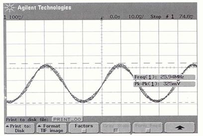
Figure 7. Output waveform from PCB Transmitter
When a wire antenna of approximately 3 feet was added to the circuit, the team was able to receive a fairly intelligible voice signal with the FM radio. Conversely, without the antenna the output signal of the transmitter could not be received.
4.2.4 Performance
Testing of the transmitter with an antenna showed promising results. With the antenna, a voice signal could be transmitted and understood intelligibly over the handheld FM radio. However, the performance of the PCB transmitter was not equivalent to that of the prototype. The prototype transmitter had a clear transmission range of approximately 10 feet without an antenna. The PCB transmission range was approximately 2 feet with a 2-3 foot long wire antenna. The prototype circuit has relatively long wires in comparison to the PCB circuit, so the performance gap could be due to this difference. These wires act as small antennas to propagate the FM signal. Therefore, future work on the PCB transmitter will include experimentation with the addition of an antenna.
RESULTS AND CONCLUIONS
5.1 FINAL EVALUATION
Given the experience of the team and the magnitude of the project, significant progress was made miniaturizing the EarTalk wireless communication system. Figure 8 shows the final FM transmitter system within an earmold. The system contains a miniature microphone, a hearing aid battery, and the transmitter circuit.
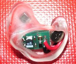
Figure 8. Final FM transmitter within earmold.
The two primary results of this project are a fully functional analog FM transmitter prototype that performs consistently and a miniaturized PCB transmitter. The transmitter on the PCB will transmit with a long antenna connected at the output. The signal can be received clearly for a short amount of time from a distance of 8-10 inches away. A significant amount of the time spent on this project involved troubleshooting the circuits. In constructing and testing both the prototype and the PCB, there were several problems encountered. Despite setbacks and unpredictable performance of the final design, the team is extremely proud of the resulting hardware and the lessons learned throughout the course of the project.
5.2 FUTURE MODIFICATIONS
In order to increase the performance of this transmitter, a more efficient antenna is necessary. Additionally, the tank circuit of the transmitter needs to be optimized in order to maintain a stable carrier frequency. More research should be done on the type of microphone that will best suit this circuit. Further investigation into communication circuits implemented on PCBs may also lead to designing a new PCB for optimal RF transmission. A higher frequency design could also help with transmission issues. Future teams should also include a mechanical engineer to design a secure and accessible battery holder.
EXPENSES
The detailed expense report below presents the total student labor costs for the duration of the project. In addition, the budget includes parts and supplies that were purchased.
Table 2. Expenses
|
1. Personnel | |||||
|
Name |
Title |
Time |
Wage |
Total |
|
|
Bryan Woolstenhulme |
CompE Student |
270 hours |
$20/hour |
$ 5,400.00 |
|
|
Erica Lively |
EE Student |
270 hours |
$20/hour |
$ 5,400.00 |
|
|
Mark Martin |
EE Student |
270 hours |
$20/hour |
$ 5,400.00 |
|
|
| |||||
|
2. Parts/Supplies | |||||
|
Item |
Cost/Item |
Quantity | |||
|
Knowles electret microphone (rectangular) |
$ 19.44 |
||||
|
Surface mount resistors, capacitors, transistors, and an inductor |
$ 29.46 |
||||
|
Various inductors, transistors, and variable capacitors |
$ 46.95 |
||||
|
1N3716 - Tunnel Diodes |
$ 90.00 |
||||
|
1N34A - Germanium Diodes |
$ 1.60 |
||||
|
"Olive Martini" FM Transmitter Schematic |
$ 10.00 |
||||
|
Prototype PC board |
$ 3.58 |
||||
|
Anti-static kit |
$ 24.99 |
||||
|
Handheld AM/FM radio |
$ 16.99 |
||||
|
6-piece precision screwdriver set |
$ 4.99 |
||||
|
Precision capacitor adjustment tool |
$ 27.16 |
||||
|
AA batteries |
$ 3.99 |
||||
|
Hearing aid batteries - size 10 |
$ 10.99 |
||||
|
Custom molded earplugs |
$ 174.99 |
||||
|
Custom PC board |
$ 257.00 |
||||
|
Subtotal |
$ 16,922.13 |
||||
|
Shipping & handling |
$ 58.71 |
||||
|
Total |
$ 16,980.84 |
||||
The team would like to extend special thanks to NIOSH and Cmdr. Chuck Kardous for funding this interesting and exciting project. Additional thanks are also due to Cmdr. Kardous for his time and helpful input. The team would also like to thank our advisor, Dr. David Egolf, for his continued support. All of his advice and encouragement have proven to be invaluable to the project. In addition, Dr. Richard Wall, Dr. Jeff Young, Dr. David Atkinson, Dr. Ken Noren, and Dr. Rick Wells provided valuable input and expertise.
1. EWM-900-FDTC Low Cost 902-928MHz Full Duplex Audio/Data Transceiver. (2004). Retrieved December 6, 2004 from https://www.radiotronix.com/datasheets/ewm-900-fdtc-datasheet.pdf .
2. Franks, J. R., Sizemore, C. W., Dunn, D. E. (1995).
3.
4. Kardous, C. A. (2003, January-February). Ear Talk: Protector & Microphone. The Military Engineer, 621, 43-44.
Oh, P.Y. (n.d.). Wireless FM Transmitter. Retrieved November 2, 2004 from the Boondog Automation Web site: https://www.boondog.com/\tutorials\rfTransmitter\rfTransmitter.htm .
Van Roon, Tony. (2003). Miniature FM Transmitter #3. Retrieved December 12, 2004 from https://www.uoguelph.ca/~antoon/circ/fmt3.htm .
7. Wuthrich, J. R.,
8. XE 3005 / XE 3006 Low-Power Audio CODEC. (2003). Retrieved December 6, 2004 from https://www.xemics.com/docs/xe3000/xe30056_datasheet.pdf .
9. XE1201A 300-500MHz Low-Power UHF Transceiver. (2002). Retrieved December 6, 2004 from https://www.xemics.com/docs/xe1200/xe1201a_datasheet.pdf .
10. XE88LC06A and XE88LC07A Ultra Low-Power Low-Voltage Radio Machines. (2004). Retrieved December 6, 2004 from https://www.xemics.com/docs/xe8000/xe88lc06a_7_datasheet.
APPENDICES
APPENDIX A-Design Functionality of Individual Digital Integrated Circuits
APPENDIX B-Design Functionality of Digital Integrated RF Transceiver Module
APPENDIX C-Additional Analog FM Transmitters
APPENDIX
D-List and Description of Surface
APPENDIX A-Design Functionality of Individual Digital Integrated Circuits

Figure A1. Block diagram of digital design #1.
A.1 Amplifier and ADC (CODEC)
After the microphone converts the user's speech, the weak electrical signal is fed through an amplifier. This amplified signal then passes to the ADC, which converts the analog signal to digital. This conversion takes place by sampling the incoming analog signal at a specific rate. The amplitude of each sample is then approximated with a binary number. Thus, the ADC produces a string of binary numbers that represent the original analog signal. The size of each binary number is typically 8 or 16 bits. Increasing the number of bits increases the accuracy or resolution of the ADC because additional bits better approximate each sample.
Further research into the amplifier and ADC revealed that many IC manufacturers combine both into a single component called a CODEC. A company called Xemics produces CODECs along with all the other necessary components for this design, aside from the microphone.
The XE3005 is a very small voice/audio CODEC made by Xemics. It operates on a supply as low as 1.8 volts and is only 6.6 x 6.6 mm in size (XE 3005, 2003, p. 32). These specifications make the XE3005 a good choice for this design.
A.2 Microcontroller
Following amplification and conversion, the digital signal passes to the microcontroller (refer to Figure 2). The role of the microcontroller is to arrange the stream of digital binary data into individual packets in preparation for RF transmission by the transceiver. This operation is also known as encoding (Wuthrich, et al., 2002, p. 8). Typically, each packet will contain an extra bit or bits called start bit(s) at the beginning to signify the start of a new packet. Following the start bits are the actual binary data bits. At the end of the packets are often stop bits to indicate the end of a data packet. The receiving end of the transmission system uses these start and stop bits to synchronize with the transmitter. In particular, the digital-to-analog converter on the receiving side uses the start bits to determine the beginning of a digital sample for conversion back to an analog signal.
The XE88LC06A is a very low-power radio microcontroller made by Xemics. With operation on as little as 2.4 volts and a size of 7.1 x 7.1 mm, it is also a good fit for this design (XE88LC06A, 2004, p. 144).
A.3 Digital RF Transceiver
The final link in the transmission chain is the digital RF transceiver. The transceiver transmits the digital data packets produced by the ADC and microcontroller to the receiving end of the transmission system via radio waves. FM transmission is the best modulation technique for this design because demodulation of the signal is much more accurate, therefore resulting in better clarity. In addition, FM transmission range is shorter than that of AM resulting in less interference. This is due to the shorter wavelength of FM waves. Therefore, FM transmission is better suited for this design.
Xemics produces very small and low power transceivers that operate in the 300-915MHz range. In particular, the XE1201A operates at 2.4 volts and is 9 x 9 mm in size (XE1201A, 2002, p. 14). These properties make it a good fit for this design.
A.4 Design Evaluation
The primary advantage of the individual IC component design is that all components can operate at 2.4 volts, well below the maximum supply voltage of 3 volts. Second, all of the components are available from a single source, Xemics. This is advantageous because the various components are designed to work together.
However, the disadvantages of this design include difficulty of implementation given the limited experience of the team and a relatively large number of components. While completion of the final system is possible, it is not feasible within the allotted time of four months. In addition, even though the sizes of the individual components are very small, the size of the final design could be large because of the number of parts involved.
APPENDIX B-Design Functionality of Digital Integrated RF Transceiver Module

Figure B1. Block diagram of digital design #2.
B.1 Transceiver Module
The integrated transceiver module performs the functions of the amplifier, ADC, and transceiver components in the first design. In this way, the module integrates several components into a single device and thus requires few external components. There are three modules identified for this design. The first module is the EWM-900-FDTC produced by Radiotronix. This audio/data module operates on 3 volts, is 30.9 x 20.8 mm in size, and transmits in the 900MHz range. It provides full duplex operation and has 56 channels (EWM-900-FDTC, 2004, p. i). Full duplex operation allows for data to be transmitted and received at the same time. The large number of channels allows for the use of a network of many individual modules as is necessary for group communication.
The other two modules are the RF900CLP and TLP 2.4G both produced by Laipac Technologies. The RF900CLP operates at 3.6 volts, is 43.6 x 39.4 mm in size, and also transmits in the 900MHz range. However, the 3.6-volt operating voltage for this module is slightly high for this design. The TLP 2.4G operates as low as 1.9 volts, is 20 x 36 mm in size, and transmits at 2.4GHz. Both of these modules are full duplex; however the TLP 2.4G is a better fit for this design than the RF900CLP due to its lower operating voltage and smaller size.
B.2 Microcontroller
Similar to the previous design, the function of the microcontroller in this design is to arrange the digital data into discrete packets in preparation for transmission. However, in this design, the microcontroller must also program the registers within the transceiver module to set the communication channel and operating modes.
B.3 Design Evaluation
The primary advantage of this design is the low number of components necessary. It requires only three components compared to five required in the first design. Considering the low component count, this design would also be easier to implement and potentially smaller than the first design. Finally, two of the three modules identified operate at the maximum voltage of 3 volts or lower. Therefore, these two modules meet the criteria for low power consumption.
Again, the disadvantage of the module design is the complexity of implementation. Even with the reduced component count, the interface between the microcontroller and the transceiver module is fairly involved. Thus, this design is not the best in terms of ease of implementation.
APPENDIX C-Additional Analog FM Transmitters
Figures C1-C3 below show three of the analog FM transmitter circuits that were tested, but not chosen as the final design. None of the circuits were functional after several rounds of initial testing.
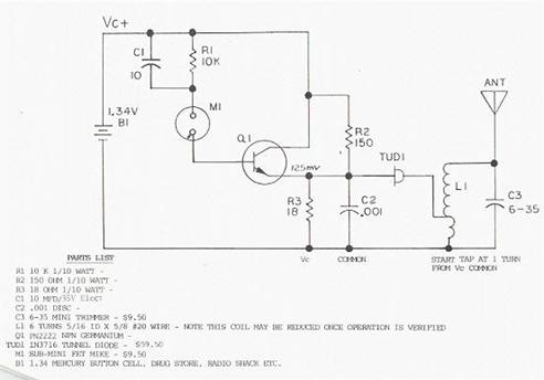
Figure C1. FM transmitter with tunnel diode.
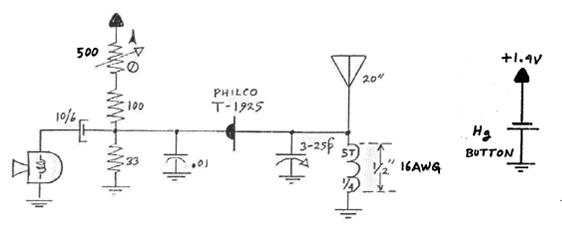
Figure C2. Tunnel diode FM transmitters.
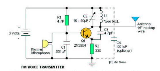
Figure C3. FM transmitter containing transistor.
APPENDIX D-Surface
After deciding on the use of surface mount components, the next step was to identify the correct parts to use for this application. Again, because size was a crucial factor, it was desirable to use small components.
Resistors were the smallest components in the circuit, while the 33uF polarized capacitor was the largest. Package size 0402 resistors were chosen because of their small dimensions (1.00 x 0.50 mm) and power rating of 62.5mW. The largest power dissipated in a resistor in the prototype circuit was only 0.504mW. Thus, 62.5mW rated resistors were more than adequate in terms of power dissipation. A further incentive for choosing the 0402 resistors was that libraries for the parts already existed in the layout software.
In addition, the 2nF and 6pF capacitors in the circuit were available in 0402 packages. These libraries were also previously built-in to the layout software.
The 33uF polarized capacitor used in the prototype circuit was a conventional thru-hole electrolytic type. However, because of the large size of this type of capacitor, the surface mount design required a much smaller type of polarized capacitor. Therefore, a smaller Tantalum Electrolytic Chip Capacitor was implemented in the PCB circuit. Luckily, this capacitor came in a standard package that was already included as a library in the layout software.
The variable capacitor was one of the most difficult parts to choose in the circuit. Many different varieties of surface mount variable capacitors are produced in varying sizes and shapes. With size in mind, the smallest variety was selected with a range from 3pF-8pF. However, adjustment of this variable capacitor proved to be a difficult task as will be mentioned later on in this report. Another drawback with this variable capacitor was that a library had to be created for it in the layout software.
Similarly, it was somewhat difficult to decide upon which transistors to use in the PCB circuit. Surface mount versions of the 2N2222 thru-hole transistors used in the prototype could not be found. Therefore, the 2N2222s were replaced with 2N3904 general purpose transistors to determine if the circuit operated correctly. The prototype operated excellent with the 2N3904s. Thus, surface mount versions of the 2N3904 thru-hole transistors were selected for the PCB design. These surface mount transistors came in the common SOT-23 package. This package was already included in the layout software.
A fixed 0.47uH surface mount inductor was chosen for the tank circuit. With the 3.0-8.0pF variable capacitor, this resulted in a theoretical frequency range of 82.08MHz - 134.03MHz. Similar to most of the other components, the package for the inductor was already present in the layout software.
Parts List:
|
Digi-Key Part Number |
Description |
|
P100LCT-ND |
Resistor - 100 OHM |
|
P3.01KLCT-ND |
Resistor - 3.01K OHM |
|
P3.32KLCT-ND |
Resistor - 3.32K OHM |
|
P121KLCT-ND |
Resistor - 121K OHM |
|
497-2478-1-ND |
Transistor - 2N3904 |
|
P11311CT-ND |
Capacitor - 33UF |
|
PCC1725CT-ND |
Capacitor - 2.200NF |
|
PCC060CQCT-ND |
Capacitor - 6.0PF |
|
490-2011-1-ND |
Variable Capacitor - 3.0-8.0PF |
|
PCD1180CT-ND |
Inductor - .47UH |
|