PIC16C84 Development System
Contents
1. Getting started
1.1 Why write a new assembler?
1.2 Software installation
2. The development cycle
3. A84, the assembler
3.1 Assembler command line
3.2 Assembler syntax
3.3 Directives
3.4 Conditional Assembly
4. P84, the programmer control software
4.1 Programmer command line
4.2 Installation and testing
5. PIC16C84 functional overview
5.1 Memory map
5.2 Special Function Registers
5.3 Configuration word
5.4 I/O ports
5.5 The timer / counter
5.6 Accessing the data EEPROM
5.7 Interrupts and interrupt service routines
6. Instruction summary
6.1 Alphabetic list of instructions
6.2 Operation/Operand matrix
6.3 Operations
6.4 Instruction execution timing
7. Tricks of the trade
7.1 Power saving with watchdog
7.2 Boolean variables and bit oriented instructions
8. RS232 Example
8.1 The circuit
8.2 The software
9. Going further
9.1 Development tools
9.2 Further information
Why develop another PIC assembler when there are others out there?
There are quite a few PIC assemblers which are readily available. Some of them are easily retrieved from Internet ftp sites or bulletin boards, others can be bought for fees ranging from a few tens to a few hundred dollars.
At the time of first writing this assembler, none of those available seemed to provide effective support for the integration of the PIC16C84's EEPROM data space. Some were liable to crash instead of giving helpful error messages. Others supported so many features and PIC variants that they were difficult to understand; even now, with a few PIC projects under my belt, I still don't fully understand some of their features.
Thus into this void, out of necessity for an assembler I could trust and understand, I wrote my own specifically for the PIC16C84. Even now that other reliable assemblers are available it still makes sense to make this assembler available. The other assemblers are packed with features and are general purpose, covering the entire PIC range, thus they are often difficult to learn and the support for PIC16C84 specific features might not be directly built in.
I focussed on creating a PIC16C84 assembler for the learner PIC programmer. The main goal for this assembler is to keep it simple to use so that you can get programming within minutes rather than days. Thus this assembler provides no unnecessary features required by parts other than the PIC16C84. It is fully capable of generating any program that the PIC16C84 can execute and can also generate programs for other 14 bit PIC16Cxx series microcontrollers; but it's with the PIC16C84 that it really shines!
I persevered because I believe this assembler serves a purpose: making the PIC technology easily accessible to the novice programmer.
Software installation is a straightforward procedure using no fancy installation procedure:
Create a directory.
Copy the files from the diskette into the directory.
If you're going to use the software from any other directories, then add the directory to the search path.
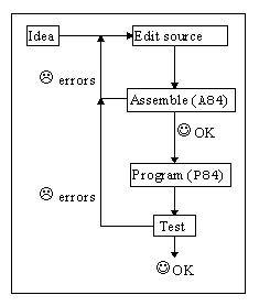
Development cycle steps
The diagram above shows the typical steps in the development of a PIC based system, or almost any embedded system for that matter.
Once you've worked out the basic ideas on how to get your system running, you need to create the assembler source code of the program. This can be done with any text editor. It is often easiest to start with an existing file and use that as a template rather than starting from scratch.
The source file is then passed through an assembler, A84.EXE, which converts the source code into object code . The assembler also performs some error checking, so it might produce some error messages if there is something that it doesn't understand. If you get error messages, then fix them and try again.
The object code is in a form which can be read by the programmer control software, P84.EXE, and can be 'burned' into the PIC. This software also performs other hardware level operations such as verification, erasing and reading of the PIC contents.
The assembler is invoked by the command line:
A84 source_file_name object_file_name
eg.
A84 DSLOCKRC.PIC DSLOCKRC.OBJ
The assembler will then read the source file and, if there are no errors, it will output some statistics and generate the object file.
This section describes the syntax used by the assembler. The main goal with this assembler was to keep the syntax simple. While this section specifies the 'rules', the best way to get to grips with how to write software is to take an existing program and modify it.
Case is of no significance except where an ASCII character is being specified between quotes. Thus, the symbols abc ABc and abC are all equivalent. However, for your own sake, choosing one representation makes your source code much easier to read. The quoted ASCII character 'A' and 'a' are not equivalent.
Numbers may be expressed in decimal, octal or hexadecimal.
Decimal numbers start with a digit in the range to
Octal numbers (base 8 numbers) start with a and must contain only the digits to . For example, equivalent to decimal. Generally, octal numbers are very infrequently used.
Hexadecimal (base 16 numbers) numbers may be expressed in sequences which starts with a digit in the range to and end with a 'H'. For example, 0abch, which is equivalent to decimal. As mentioned before, the all these are case insensitive.
Single ASCII characters may be specified by enclosing them between two quote ( ) characters. For example 'A'. The quote character may be quoted by writing . Only one character may be quoted at a time.
Symbols include labels and equivalence symbols. These must start with the underscore character ' ' or an alphabetic character 'A' to 'Z'. The rest of the symbol may contain any other printing character except the period ' ', comma ' ' and semi-colon ' ' characters which have special meanings.
To declare a symbol it must start in the first character on a line. If the line contains anything but an EQU, DBEE or RB directive, then it is assumed to be a label for the next instruction.
Unless being specified as an ASCII character ( ), a semicolon signifies the first character of a comment. The assembler ignores all the text to the end of the line.
A bit selector is the parameter to the bit oriented commands. It is composed from two logical parts: a byte address and the address of the bit within the byte. These are jointed into a single syntactic unit with the period (' ') character. The format for this is byte_address.bit_address. Blanks are not allowed between the two address parts and the period. The byte_address is a seven bit value and can be any word or byte value (which will be trimmed down to 7 bits if need be). The bit_address is a value in the range to . Other values are illegal.
Examples:
Z equ STATUS.2 ; the Zero bit in the status register.
btfsc Z ; use it in a
bit oriented instruction
btfsc STATUS.2 ; does the same
thing
btfsc 3.2 ; also does the
same thing
If an assembler instruction requires more than one argument, then the arguments are delimited (separated) by a comma. '
Directives are special instructions to the assembler. They control the operation of the assembler and do not result in machine code being produced for the target processor. The assembler supports the following directives.
|
Directive |
Function |
|
CONFIG |
Set configuration word |
|
DBEE |
Define byte in EEPROM |
|
ECHO |
Echo text line |
|
EQU |
Equate symbol to value |
|
INCLUDE |
Include specified text file into assembly |
|
ORG |
Set Program memory address |
|
ORGDATA |
Set RAM memory address |
|
ORGEEDATA |
Set data EEPROM address |
|
RB |
Reserve byte in RAM |
|
RBEE |
Reserve byte in EEPROM |
Form
CONFIG <config_val>
The CONFIG directive sets the configuration word to the specified value. This value is then used to configure the PIC16C84.
Examples
config 0ffh ;
no protection, power up timer enabled,
;
watchdog enabled, RC oscillator
Form
[symbol_name] DBEE initialisation_value
The DBEE directive is very similar to the RBEE directive mentioned below. It increments the EEPROM data space pointer by one and initialises the byte to the specified value. The specified value will be programmed into the PIC16C84 if the data EEPROM is programmed. Also, if a symbol name is specified, a symbol will be generated for the EEPROM data space pointer value before it is incremented.
Examples
ee_char DBEE 'A' ; start it off with 'A'
ee_number DBEE 0 ; start off with zero
Form
ECHO This text will be displayed
The ECHO directive outputs the text in the line on the standard output. This is often useful as a confirmation when conditional assembly is being used.
Example
echo Assembling timer module
Form
symbol_name EQU assigned_value
The EQU directive is used to assign a particular value to a symbol. When the symbol is encountered later during the assembly process, the equated value will be substituted. The value that is being assigned must be known when the EQU directive is encountered.
Examples:
MaxCount EQU 200
LastValue EQU MaxCount ; equivalent to LastValue equ 200
FirstAlpha equ 'A' ; FirstAlpha now equivalent to ASCII
; value
for A (65 decimal)
Z equ STATUS.2 ; the Zero bit in the status register.
Form
INCLUDE filename
The INCLUDE directive includes the contents of the named file into the assembly sequence. When the end of the included file is reached, then the assembler continues assembly on the next line of the file that did the include. Include files may be nested up to 10 files deep.
Example
INCLUDE PICREG.INC
Form
ORG address_value
The ORG directive sets the value of the next address to be assigned to the next instruction that is assembled. It is usually sufficient to allow the assembler to take care of address assignment. It is suggested that the ORG directive be used to assign the address of start up code and the interrupt code. The assembler will detect any attempts to assign the same address to more than one instruction.
Example
ORG Program_Start
ORG Interrupt_Start
Form
ORGDATA address_value
The ORGDATA directive sets the value of the next data space address to be assigned by the RB directive. The same address may be multiply assigned, so be cautious what you do! The default start up value is 0CH (12 decimal) which is the first byte of RAM on the 16C84.
Example
ORGDATA Ram_Base
Form
ORGEEDATA address_value
The ORGEEDATA directive sets the value of the next EEPROM data space address to be assigned by the DBEE or RBEE directives. The same address may be multiply assigned, so be cautious what you do!
Example
ORGEEDATA 5
Form
[symbol_name] RB [optional number of bytes, default 1]
The RB directive increments the data space pointer by the specified number, default one if not specified. Also, if a symbol name is specified, a symbol will be generated for the data space pointer value before it is incremented.
Examples
rx_char RB
rx_buff RB buff_size
Form
[symbol_name] RBEE [optional number of bytes, default 1]
The RBEE directive increments the EEPROM data space pointer by the specified number, default one if not specified. Also, if a symbol name is specified, a symbol will be generated for the EEPROM data space pointer value before it is incremented.
Examples
ee_char RBEE
ee_buff RBEE buff_size
Conditional assembly provides a mechanism to select what parts of a file are to be assembled and which are to be ignored.
|
Directive |
Description |
|
IF <symbol> |
If the value equated to the symbol is not zero, then assemble the following section |
|
IFDEF <symbol> |
If the symbol is defined, then assemble the following section |
|
IFNDEF <symbol> |
If the symbol is not defined, then assemble the following section |
|
IFNOT <symbol> |
If the value equated to the symbol is zero, then assemble the following section |
|
ELSE |
If nothing in this conditional body has been assembled, then assemble this section, otherwise skip it. Can only be the last section in the conditional body. |
|
ELSEIF <symbol> |
If nothing in this conditional body has been assembled, then assemble this section if the symbol equates to a non-zero value, otherwise skip it. |
|
ELSEIFDEF <symbol> |
If nothing in this conditional body has been assembled, then assemble this section if the symbol is defined, otherwise skip it. |
|
ELSEIFNDEF <symbol> |
If nothing in this conditional body has been assembled, then assemble this section if the symbol equates to a non-zero value, otherwise skip it. |
|
ELSEIFNOT <symbol> |
If nothing in this conditional body has been assembled, then assemble this section if the symbol equates to a non-zero value, otherwise skip it. |
|
ENDIF |
End of conditional body |
The following rules apply to constructing a body of conditional assembly code:
All conditional bodies begin with an IFxxx and end with ENDIF
Zero or more ELSEIFxxx code sections can follow
At most one ELSE code section can be placed as the last code section to a code body
Conditional bodies can be nested. The limit is 10 nesting levels.
As an example:
IFDEF foo
; assemble this if the symbol foo is defined
ELSEIFDEF bar
; assemble this if foo is not defined and bar is defined
ELSEIFDEF fred
; assemble this if foo and bar are not defined and fred is defined
ELSE
; assemble this if none of foo, bar or fred are defined.
ENDIF
The programmer control software is invoked by the following command line:
P84 flags object_file_name
eg.
P84 /E /LA /VA DSLOCKRC.OBJ
This command line first erases the PIC then loads all of the program, data EEPROM and configuration and verifies them using the object code in the file DSLOCKRC.OBJ.
|
/E |
Erase the PIC. |
|
/P1, /P2 |
Sets the programmer communication port to LPT1 or LPT2. The setting is stored in the file P84CFG.DAT in the same directory as P84.EXE and will be use in subsequent operations until overridden by specifying this option again. |
|
/T |
Test the programmer hardware. |
|
/RP |
Read program memory into specified file. |
|
/RD |
Read EEPROM data memory into specified file. |
|
/RC |
Read configuration fuses into specified file. |
|
/RA |
Read all of program memory, EEPROM data memory and configuration fuses into specified file. |
|
/LP |
Load program memory from specified file. |
|
/LD |
Load EEPROM data memory from specified file. |
|
/LC |
Load configuration fuses from specified file. |
|
/LA |
Load all of program memory, EEPROM data memory and configuration fuses from specified file. |
|
/VP |
Verify program memory against specified file. |
|
/VD |
Verify EEPROM data memory against specified file. |
|
/VC |
Verify configuration fuses against specified file. |
|
/VA |
Verify all of program memory, EEPROM data memory and configuration fuses against specified file. |
The commands are not necessarily executed in order in which they are specified in the command line, but rather in the order which seems to make the most sense. Erases always happen first. If both load and verify operations are specified, the program and data EEPROM are first loaded and verified, then the confguration fuses are loaded and verified. The reason for this ordering is that this allows the program and data EEPROM to be verified before the code protection is enabled. Once the code protection is enabled, then the programmer can no longer verify the PIC against the object file.
The following outline the basic steps for installing the programmer:
Install the programmer by connecting it to a printer port (LPT1 or LPT2) and a suitable power source.
Configure the programmer
control software with the command:
P84 /P1 or P84 /P2
according to which printer port you used.
Test the programmer and its
configuration by running the following command:
P84 /T
It is important to ensure that there is no PIC in the programmer during testing. Pressing 'C' will continue with the test, any other key will abort the test. The software then displays sixteen combinations of signals, press Enter to move to the next selection. Note that the Data and Clock signals are only valid when Power is on. The LED will also be lit when power is on. Finally an automatic input test is performed to ensure that the input data path is functioning correctly. The signals can be measured from the following pins:
|
Pins |
Description |
Off |
On |
|
Ground |
0V |
0V |
|
|
Programming voltage |
0V |
12-14V |
|
|
Clock |
0V |
5V |
|
|
Data |
0V |
5V |
|
|
Power |
0V |
5V |
|
|
No connection |
The PIC16C84's memory map can be separated into four areas:
Program EEPROM space
Data RAM space
Data EEPROM
Stack
The PIC16C84 supports storage for up to 1024 instructions. This is quite small, but the PIC's compact instructions make this go a long way.
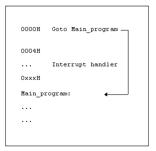
Two instruction addresses have special uses:
|
0000h |
This is the reset vector. When the PIC is reset or powered up, it starts executing here. |
|
0004h |
This is the interrupt vector. When the PIC detects an interrupt, it starts executing here. |
Since you can't fit much of a program in four instructions, the normal way to lay out a program is something like:
The PIC16C84 supports 36 bytes of RAM. Is that ALL? Yep, in these days of multi-megabyte PCs, 36 bytes might seems far too small to do anything useful. However using the correct software design approach can squeeze the most out of it.
For some reason lost in the mists of time, Microchip called data memory bytes "files". It really just means memory.
The data memory space is shared with the special function registers according to the following table.
|
Range |
Usage |
|
00H-0BH |
Special function registers |
|
0CH-2FH |
Data RAM |
|
30H-7FH |
Not implemented |
|
80H-8BH |
Special function registers |
|
8CH-AFH |
Maps to RAM in 0CH-2FH |
|
B0H-FFH |
Not implemented |
The PIC16C84 supports an 8 deep call stack which means that it automatically keeps track of up to 8 levels of subroutine or interrupt calls.
Well, deep isn't really the word, it's actually arranged as a circular list. This means that if you overflow the stack, it writes over the oldest entries and keeps track of the 8 most recent calls. Of course no sensible software should do something like this.
Unlike many other microcontrollers, the stack is not part of the RAM, so you can't access it. This has some advantages; you can't corrupt the stack by writing to it and it makes those 36 bytes of RAM go a lot further than they would on other microcontrollers.
The PIC16C84 supports 64 bytes of data Electrically Erasable Programmable Read Only Memory (whew, I think I'll stick to EEPROM!). This is a particularly useful feature as this type of memory retains information even when power has been removed.
However, EEPROM has certain limitations. While it can be read at the same speed as RAM, writes take a while longer (about 10 milliseconds). Also, there is a limit to how often each memory position can be overwritten.
Although not really memory, the special function registers are mapped into the PIC's data memory address space as if they were ordinary memory cells.
|
Address |
Register |
Function |
|
00h,80h |
INDF |
Indirect data register |
|
01h |
TMR0 |
8 bit real-time clock/counter |
|
02h,82h |
PCL |
Lower order 8 bits of program counter |
|
03h, 83h |
STATUS |
Status register |
|
04h,84h |
FSR |
Indirect address register (file select register) |
|
05h |
PORTA |
Port A |
|
06h |
PORTB |
Port B |
|
08h |
EEDATA |
EEPROM data register |
|
09h |
EEADR |
EEPROM address register |
|
0Ah,8Ah |
PCLATH |
Write buffer for program counter bits 12..8. |
|
0Bh,8Bh |
INTCON |
Interrupt control register |
|
81h |
OPTION |
Option register |
|
85h |
TRISA |
Port A direction control register |
|
86h |
TRISB |
Port B direction control register |
|
88h |
EECON1 |
Data EEPROM control register 1 |
|
89h |
EECON2 |
Data EEPROM control register 2 |
|
Address |
Power up |
Other resets |
|
03h, 83h |
00011xxx |
000??uuu |
The status register contains the arithmetic status, reset status and page select bits for the PIC.
|
Bit |
Symbol |
Function |
|
C |
Carry bit. |
|
|
DC |
Digit carry bit |
|
|
Z |
Zero bit. |
|
|
PD |
Power down
bit: |
|
|
TO |
Time out
bit: |
|
|
RP0 |
Register
bank select bits: |
|
|
IRP |
Indirect
register bank select |
The carry bit, C, is modified by arithmetic instructions and the rotate instructions. The digit carry bit, DC, has a similar function except it shows when carries have been performed between the two four-bit nibbles. DC is not affected by the rotate instructions.
The zero bit, Z, is set (1) when the result of the last arithmetic or logical instruction is zero.
The PD and TO bits can be used to determine the state of the PIC. These work together as follows:
|
TO |
PD |
Cause |
|
Watchdog time-out wake from sleep |
||
|
Watchdog reset during normal operation |
||
|
Hardware reset during sleep or woken by interrupt during sleep |
||
|
Power on reset or hardware reset during normal operation. |
This is especially important when using the watchdog timer. For example, if a watchdog timer expired during normal operation, then the PIC will reboot with TO=0 and PD=1. This condition can be detected at start up and handled as a system failure.
The PIC architecture supports up to 512 bytes of data memory. This is more memory than can be addressed by the 7 bit "file" addresses used by the PIC instructions. The PIC architecture overcomes this problem by splitting the address space into four banks of 128 bytes each. The page select bits, RP0 and RP1, select which bank is currently being accessed. Since the PIC16C84 only implements two banks, RP0 is sufficient to perform bank switching and RP1 serves no purpose here. In fact, RP1 could be used for general purpose storage (wow, a whole bit!), however don't do this if your programs are going to be ported over to PICs where RP1 is required for bank selection.
Similarly, the PIC architecture requires an extra bit for indirect addressing. The indirect addresses are 8 bits long which means that an extra bit is required to access the PIC architecture's entire RAM address range. This bit is IRP. Again, since the PIC16C84 only implements part of the address range, IRP is not needed in this role and can be used for other purposes (gee, another bit!) with the same precautions as RP1
|
Register |
Address |
Power up |
Other resets |
|
INDF |
00h, 80h | ||
|
FSR |
04h, 84h |
xxxxxxxx |
uuuuuuuu |
INDF is not a real register, but a 'window onto other memory locations. These two special function registers implement the PIC's indirect data access mechanism. This mechanism is extremely simple to use:
Load FSR, the file select register, with the address of the location to be accessed.
Accesses to INDF, the indirect data register, access the location at the address specified in FSR
At first glance you might ask "Why not access the data directly?". Well, there are two very good uses for this mechanism:
If you need to perform an operation to a sequence of locations, then the you can load FSR with the first address, then increment FSR each time you go through the loop, thus accessing the next location. An example of this idea, though accessing EEPROM data through EEADR and EEDATA, is used in the example lock code.
Since the indirect addresses in FSR are eight bits wide, they can access the entire PIC16C84 data range. Using this mechanism provides an alternative to using page selection with RP0 to access data in the upper page.
|
Address |
Power up |
Other resets |
|
81h |
The option register contains the timer options, interrupt edge and Port B pull-up enable bits.
|
Bit |
Symbol |
Function |
|
PS0 |
Timer
prescaler |
|
|
PSA |
Prescaler
assignment: |
|
|
T0SE |
Timer 0
source edge select bit: |
|
|
T0CS |
Timer 0
clock source select bit:: |
|
|
INTEDG |
Interrupt
edge select bit: |
|
|
RBPU |
Port B
pull-up control bit: |
The prescaler assignment bit, PSA, and the prescaler divisor selectors, PS2 PS1 and PS2, control the operation and usage of the prescaler. The prescaler can be assigned to either the watchdog timer or to Timer 0.
T0SE and T0CS control the clock source for Timer 0.
INTEDG selects whether external interrupts are triggered on the rising or falling edge of the RB0/INT pin.
The RBPU bit controls the Port B pull-ups. The Port B pull-ups are effectively high value resistors. This feature can simplify circuits where Port B is used for active low inputs. Normally a resistor is required to provide the pull-up, but this is not required if the internal pull-ups are enabled.
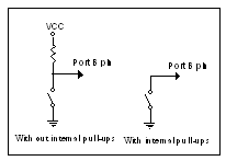
Apart from being accessed at the address 81H, the OPTION special function register can be set by the special OPTION instruction. Microchip strongly recommends that this instruction is not used as they do not guarantee that they will support it in future PICs.
|
Name |
Address |
Power up |
Other resets |
Role |
|
PCL |
02h, 82h |
Bits 7..0 of program counter |
||
|
PCLATH |
0AH, 8AH |
Bits 12..8 latch for program counter loads. |
PCL and PCH hold the contents of the PIC's 13 bit wide program counter. The program counter is the reference to the next instruction to be executed. PCL is directly accessible, however PCH is not. The value of PCH can be controlled via PCLATH which is accessible. The way that this works is as follows.
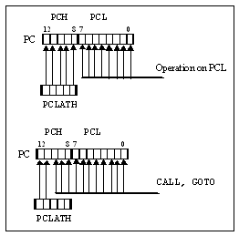
If the program counter is modified by executing a CALL or GOTO instruction, then the 11 bit address operand is loaded into bits 10..0 of the PC and bits 4..3 of PCLATH are loaded into bits 12..11 of the program counter.
If the program counter is modified by an instruction with PCL as the destination, then bits 12..8 of the program counter is loaded from bits 4..0 of PCLATH.
Why would anybody want to modify the program counter in such a way? Well it provides a mechanism for performing computed GOTOs or table look-ups. There are quite a few gotchas in doing this, and I strongly suggest that you read the Microchip application note, AN556, on this subject or be prepared to experiment a bit.
The configuration word is not a special function register, but a set of configuration fuses. It cannot be modified by software, only by reprogramming (and thus reconfiguring) the PIC16C84.
|
Bit |
Symbol |
Function |
|
FOSC0 |
Oscillator selection bits: |
|
|
WDTE |
Watchdog timer enable: |
|
|
PWRTE |
Power up Timer enable: |
|
|
CP |
Code protect bit: |
|
|
Not implemented (read as 1) |
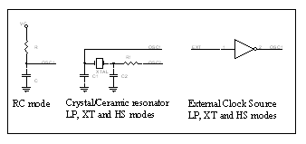
The FOSC0 and FOSC1 bits set the oscillator type. RC oscillators use a resistor-capacitor network to determine the oscillator frequency. LP, XT and HS modes all work with an external crystal or may be driven from an external oscillator. The following table shows the permitted oscillator type/frequency combinations.
|
Oscillator type |
PIC16C84-04 |
PIC16C84-10 |
|
RC |
Up to 4MHz |
Up to 4MHz |
|
XT |
Up to 4MHz |
Up to 4MHz |
|
HS |
Up to 4MHz |
Up to 10MHz |
|
LP |
Up to 200kHz |
Don't use |
Note that the HS mode has tighter voltage tolerances (4.5V to 5.5 V) than the other modes (4.0V to 6.0V).
The following diagram shows the suggested oscillator circuitry for the various modes
The WDTE flag controls whether or not the watchdog timer is enabled. I highly recommend that you do use the watchdog timer as it can help to make a product more reliable as it can help prevent the PIC getting stuck in a strange state caused by a programming error ora power glitch.
Enabling the power up timer with the PWRTE flag makes power up starts more reliable. It only adds a short time to the power up period and I would suggest that you use it in all cases except where the slight power up delay cannot be tolerated.
Setting CP, the Code Protect bit, to 0 protects the program code and EEPROM data from being read by external means (like a programmer) in any meaningful way. This helps to keep your code and information safe from prying eyes. However, be warned, as with any form of security, there might be loop holes. If CP is reprogrammed to 1, then all the program and data EEPROM memory is erased.
The PIC16C84 has thirteen I/O pins arranged as two bytes: PORTA (bits RB4 RB0) and PORTB (bits RB7 RB0). In normal operation all of these conform to TTL input levels, except for RA4 which accepts Schmitt trigger input levels.
The I/O pins can be accessed by byte-wise operations on PORTA or PORTB special function registers, or by bit-wise operations on their individual bits labelled RA4 RA0 and RB7 RB0
The input or output directions of the I/O lines are controlled by the TRISA and TRISB special function registers. If the corresponding bit in the TRISx is 1, then that pin is an input pin, otherwise it is an output pin. At power up, all pins are inputs.
The TRISx special function registers can be accessed by convention means or by a special TRIS instruction. Microchip warn against using the TRIS instruction as it might not be supported in other PICs.
The DSLOCKRC.PIC software provides an example of how the I/O ports are used. Note especially how the bi-directional I/O operations are done on the 1-wire bus.
The PIC16C84 has a single flexible timer/counter module with the following features:
Eight bit incrementing counter.
Read/write accessible via the TMR0 special function register.
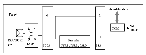
Eight bit programmable prescaler which can be assigned to either the counter or to the watchdog timer.
Selectable to count the PIC's internal clock or transitions on the RA4/T0CKI pin. Selectable to count on leading or falling edge of the RA4/T0CKI pin.
Generates an interrupt.
The diagram below shows the configuration options for the timer module.
The timer is shut off when the PIC is asleep. This also means that the PIC cannot use a timer interrupt to wake from a sleep.
If the prescaler is being used with the timer, then any operations which write to TMR0 will also clear the value in the prescaler. The value in the prescaler counter is not readable or writeable.
Most PIC variants have some or other special feature. The PIC16C84 has EEPROM program and data memory.
Since the EEPROM data memory is not directly mapped into the PIC's address space, it is accessed via four special function registers.
|
Address |
Power up |
Other resets |
|
09h |
xxxxxxxx |
uuuuuuuu |
The EEADR register holds the address of read or write operations to the data EEPROM. There are only 64 bytes of EEPROM data, so only six bits of the address are actually used. However, Microchip suggest that bits 7 and 6 are always kept at zero since the PIC draws a bit more current when these are set. The extra current is not too great, only about 250 mA.
|
Address |
Power up |
Other resets |
|
08h |
xxxxxxxx |
uuuuuuuu |
The EEDATA register is used as 'proxy' for the EEPROM memory. A read operation reads the data EEPROM at the address specified in EEADR into the EEDATA register. Likewise, the write operation writes the value from EEDATA into the address specified in EEADR
|
Address |
Power up |
Other resets |
|
88h |
---0x000 |
The EECON1 register contains EEPROM access control bits.
|
Bit |
Symbol |
Function |
|
RD |
Read control bit. Can be
set to 1 (not 0) by software. Set to 0 by hardware. |
|
|
WR |
Read control bit. Can be
set to 1 (not 0) by software. Set to 0 by hardware when the write operation
is complete. |
|
|
WREN |
Write enable bit: |
|
|
WRERR |
EEPROM error flag: |
|
|
EEIF |
EEPROM write complete
interrupt flag: 1: The write operation has completed. |
|
|
Not implemented. Read as 0. |
Setting the RD flag initiates an EEPROM read operation which takes one instruction cycle.
Setting the WR flag initiates an EEPROM write operation. The WR flag remains set until the write operation is complete, when it is cleared by the hardware.
The WREN flag is used to prevent erroneous writes to the EEPROM. It is advisable to keep to keep write access disabled except when actually writing to the data EEPROM. This helps to protect your data.
The WRERR flag indicates whether the last operation was successful.
The EEIF flag is set when the EEPROM write completes. By enabling EEIE and GIE, this flag generates an interrupt when the write operation is complete. Using an interrupt to detect a write complete is more complex, but does allow EEPROM data writing to be performed in background.
|
Address |
Power up |
Other resets |
|
89h |
The EECON2 register is not a physical register, but must be accessed as part of the EEPROM write 'magic sequence'. I have a hunch that it somehow controls an internal charge pump circuit which generates a high voltage needed for EEPROM writes.
The following code snippet shows how the EEPROM data memory can be accessed. This code is rather simple and waits until the EEPROM write is complete before returning. In many situations this is sufficient. However, the write operation takes about 10 milliseconds which might be too long to hang around waiting for some applications. This problem is overcome by using the EEPROM write complete interrupt or by periodically checking the WR bit.
; place byte to be written in EEDATA and the data EEPROM address in EEADR
; then call EEREAD
eeread
bsf rp0 ; selects upper memory page
bsf rd ; causes an EEPROM read
bcf rp0 ; go back to lower memory page
return
; place EEPROM address in EEADR, call EEWRITE to retrieve the byte at
; that address
eewrite
bcf gie ; disable interrupts during this sequence
btfsc gie ; check that it got disabled
goto eewrite ; try again if not
bsf rp0 ; select upper memory page
bsf wren ; enable EEPROM writes
bcf eeif ; clear the EEIF flag
;; the 'magic sequence' must be executed exactly as shown with
;; interrupts disabled to prevent other instructions from
;; sneaking in.
movlw 55h ; Magic write sequence
movwf eecon2 ; Magic write sequence
movlw 0AAh ; Magic write sequence
movwf eecon2 ; Magic write sequence
bsf wr ; Magic write sequence
bsf gie ; re-enable interrupts
nop ; allow a short settling time (needed?)
wait_wr_done
clrwdt ; prevent watchdog timeouts during the write
btfsc wr ; Is the write complete?
goto wait_wr_done ; No. Wait some more
bcf rp0 ; Yes, go back to lower memory page
return
If your application is not using interrupts, then you do not need to have the interrupt protection code.
Unlike the earlier 12-bit PICs, the more modern 14-bit PICs, including the 16C84, support interrupts. Although using interrupts may seem a little daunting at first, they can greatly simplify a microcontroller program when used correctly.
|
Address |
Power up |
Other resets |
|
0Bh,8Bh |
0000000x |
The interrupt control register, INTCON, holds most of the interrupt control bits. In fact, only EEIF, the EEPROM write complete interrupt flag, is held elsewhere.
|
Bit |
Symbol |
Function |
|
RBIF |
Port
B change interrupt flag: |
|
|
INTF |
External
interrupt flag: |
|
|
T0IF |
Timer 0 interrupt flag: 1:
Timer 0 has overflowed |
|
|
RBIE |
Port
B change interrupt enable: |
|
|
INTE |
External
interrupt enable: |
|
|
T0IE |
Timer
0 interrupt enable: |
|
|
EEIE |
EEPROM
write complete interrupt enable: |
|
|
GIE |
Global
interrupt enable: |
The astute reader might have noticed a pattern emerging here. For each interrupt type there is a flag (xxxF) and an enable bit (xxxE). Hang on -- where's EEIF? Well since there are only eight bits in a byte, and GIE really belongs in this byte too, the EEIF flag resides in the EECON1 register.
A warning about EEIF. It is in the upper memory page, so you may need to perform some bank switching to access it.
Note: The flags are only set by hardware and are never cleared by hardware. The programmer (that's you!) must ensure that they are cleared in software to ensure that the interrupts function correctly.
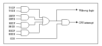
The PIC16C84 can process interrupts from four sources, identified by their associated xxIF flags:
T0IF: Depending on the current options, Timer 0 is incremented by the PIC's internal clock or by counting transitions on the TRA4/T0CKI pin. This flag is set by hardware whenever the eight bit timer value overflows and goes back to zero.
INTF: This flag is set by hardware whenever an interrupt is detected on the RB0/INT pin.
RBIF: This flag is set by hardware whenever any of RB7 RB6 RB5 or RB4 pins change state.
EEIF: This flag is set by hardware when a data EEPROM write completes.
All the xxIF and xxIE flags are cleared by software. The GIE flag is automatically restored by executing the RETFIE instruction. In fact that's the only difference between the RETFIE and RETURN instructions.
When the PIC starts executing the interrupt service routine, it automatically disables GIE, the global interrupt enable flag. If this was not done, then the PIC would start executing the interrupt service routine again, and again, and again... and you'd be in a horrible mess since the stack would soon fill up and the interrupt would never actually get processed; by now I'm sure you've guessed that the program will no longer perform any useful function. You can simulate this effect by taking an interrupt service routine and immediately re-enabling the GIE flag by adding BSF GIE as the first line in the interrupt service routine. If you do this, remember to take it out again!
Likewise, ensure that you clear the xxIF or xxIE flag during the execution of the interrupt service routine, otherwise the interrupt service routine will be re-executed as soon as the GIE flag is enabled by the RETFIE instruction, probably not what you want to happen.
One of the most important things about interrupts are that they run in background, so they should only run for a short time before returning. If you need to perform long sequences of operations in background, then these can be broken up into many short sequences which are executed by a state machine.
When an interrupt returns, the interrupted code should carry on as if nothing happened (except that a little time elapsed). In particular this means that the W and Status registers must not be altered. You might also need to save and restore FSR if indirect addressing is used in the interrupt service routine.
Of course the execution of anything but the most trivial (and useless) interrupt service routine will result in changes to the W and Status registers, particularly to the Z flag. Thus, we need to save the state of these registers at the beginning of the interrupt service routine, then restore them just before returning.
This also serves the purpose of saving the RP0 flag so that it can be restored at the end of the interrupt.
On most processors this can be achieved by pushing the registers onto a stack, then popping them off later. The PIC, however, has no stack and we thus need to find some other trick.
Well the way it is achieved is as follows:
w_save rb
status_save rb
org interrupt_start
; Magic sequence to save W and Status so that they can be restored
; at the end of the interrupt service routine.
; They *must* be executed before any instructions that modify Status or W
movwf w_save
movf status,w
bcf rp0 ; if in upper page, then flips back
; to lower page for interrupt execution
movwf status_save
; process the interrupt here
; Even more magic sequence to restore w and status registers
; before terminating the interrupt service routine
movf status_save,w
movwf status
swapf w_save,f
swapf w_save,w
retfie ;; end of interrupt service routine
;; restores GIE, the global interrupt enable flag
Why is it done this way? Well virtually any other sequence of instructions would modify the status register. If you look at the table of instructions, you will see that using a movf instead of the two swapf instructions would modify the status register.
There is a bit of trickiness in the way the PIC handles the GIE flag. It might seem that all that is required to disable interrupts is to clear the GIE flag with:
BCF GIE ; sets the global interrupt enable bit to zero
Well yes, and no! If you are sure that no interrupts will occur while this instruction is being executed, then this will work. However, due to the way the PIC processes interrupts, the following can occur.
If the interrupt happens while the above instruction is being executed, then the PIC may detect the interrupt and decide to respond to it because GIE is still enabled. Once the instruction has completed execution, GIE is disabled, but the PIC has already decided to execute the interrupt service routine, so it goes ahead and executes it. When the interrupt service routine completes it executes a RETFIE instruction and the GIE is re-enabled. Luckily there is a solution to this problem, though it isn't at all elegant.
NoInterrupts ; code to safely disable interrupts
BCF GIE ; disable the interrupt
BTFSC GIE ; check if GIE is still disabled
GOTO NoInterrupts ; it isn't, so try again
Most of the tricky bits with interrupts are mentioned above. I'll summarise the worst ones again here:
Make sure that you enable the GIE and appropriate xxIE flags to allow interrupts to function.
Don't enable the xxIE flags for interrupts which you are not handing in the interrupt service routine.
Remember to clear the appropriate xxIF flags during the execution of the interrupt service routine.
Re-enable GIE before leaving the interrupt service routine, preferably by executing RETFIE
Remember that the EEIF flag is in the upper memory page so RP0 must be set to access it directly.
If an interrupt occurs while RP0 is set, then the interrupt will execute with all direct access operations accessing the upper memory page. For this reason, it is normally easiest to clear RP0 at the start of the interrupt service routine to ensure that accesses are made to the lower memory page. If the STATUS register is saved before this is done and restored at the end of the interrupt service routine then the RP0 value, which is part of the STATUS register, will also be restored.
This section described the PIC16C84's instruction set.
|
Instruction |
Function |
Flags modified |
|
ADDLW k |
Add literal to W |
C, DC, Z |
|
ADDWF f,d |
Add W to f |
C, DC, Z |
|
ANDLW k |
AND W with literal |
Z |
|
ANDWF f,d |
AND W with f |
Z |
|
BCF f.b |
Clear specified bit |
None |
|
BSF f.b |
Set specified bit |
None |
|
BFTSC f.b |
Test specified bit, skip if clear |
None |
|
BTFSS f.b |
Test specified bit, skip if set |
None |
|
CALL k |
Call subroutine |
None |
|
CLRF f |
Clear f |
Z |
|
CLRW |
Clear W |
Z |
|
CLRWDT |
Clear watchdog timer |
TO, PD |
|
COMF f,d |
Complement f |
Z |
|
DECF f,d |
Decrement f |
Z |
|
DECFSZ f,d |
Decrement f, skip if zero |
None |
|
GOTO k |
Go to address |
None |
|
INCF f,d |
Increment f |
Z |
|
INCFSZ f,d |
Increment f, skip if zero |
None |
|
IORLW k |
Inclusive OR W with literal |
Z |
|
IORWF f,d |
Inclusive OR W with f |
Z |
|
MOVF f,d |
Move f |
Z |
|
MOVLW k |
Move literal into W |
None |
|
MOVWF f |
Move W to f |
None |
|
NOP |
No operation |
None |
|
OPTION |
Set option |
None |
|
RETFIE |
Return from interrupt |
None |
|
RETLW k |
Load literal into W and return |
None |
|
RETURN |
Return from call |
None |
|
RLF f,d |
Rotate left through carry |
C |
|
RRF f,d |
Rotate right through carry |
C |
|
SLEEP |
Enter standby mode |
TO, PD |
|
SUBLW k |
Subtract W from literal |
C, DC, Z |
|
SUBWF f,d |
Subtract W from f |
C, DC, Z |
|
SWAPF f,d |
Swap nibbles in f |
None |
|
TRIS f |
Set port direction bits |
None |
|
XORLW k |
Exclusive OR W with literal |
Z |
|
XORWF f,d |
Exclusive OR W with f |
Z |
The above is the entire instruction set for the PIC16C84. Compared with most other microcontrollers there are only few instructions, but it is still a formidable list to remember. However, if you look at the instructions, you will see that many instructions look very similar and by classifying them, as shown below, it is a lot easier to learn them.
|
Operation |
Literal |
"File" |
"File"/ |
Bit selector |
Code Address |
None |
|
Add |
ADDLW |
ADDWF |
||||
|
Subtract |
SUBLW |
SUBWF |
||||
|
And |
ANDLW |
ANDWF |
||||
|
Or |
IORLW |
IORWF |
||||
|
Xor |
XORLW |
XORWF |
||||
|
Complement |
COMF |
|||||
|
Increment |
INCF |
|||||
|
Decrement |
DECF |
|||||
|
Rotate left |
RLF |
|||||
|
Rotate right |
RRF |
|||||
|
Branch |
INCFSZ |
BTFSC |
GOTO |
|||
|
Call |
CALL |
|||||
|
Return |
RETLW |
RETURN |
||||
|
Bit Modify |
BCF |
|||||
|
Move |
MOVLW |
MOVWF |
MOVF |
|||
|
Clear |
CLRF |
CLRW |
||||
|
Nibble swap |
SWAPF |
|||||
|
No operation |
NOP |
|||||
|
Special |
CLRWDT |
|||||
|
Direction |
TRIS |
There are six basic operand types:
Literal: All these instructions are easily identified as they end with the letters LW. These instructions use the literal value and operate on the contents of the W register, leaving the results in the W register. For example:
ADDLW 5 ; adds 5 to W
MOVLW 10; sets W to 10
"File": The "file" instructions all take the address of the memory as a parameter. In many ways, this is just a form of "file"/destination, where the destination is meaningless. File addresses are always seven bits, however eight bits are required to form the complete address. The eighth bit is specified by RP0, the register page select bit. For example:
MOVWF x; move the value in the W register to x
CLRF x; set x to zero
"File"/destination: The "file" instructions all take the address of the memory as the first parameter and a destination bit as the second parameter. The destination bit dictates whether the results or the operation are stored at the specified memory address or in the W register. For example:
ADDWF x,f; adds x and W, placing the result in x
ADDWF x,w; adds x and W, placing the result in W
SWAPF x,f; swap the nibbles in x, placing the results in x
SWAPF x,w; swap the nibbles in x, placing the results in W
Bit selector: All these instructions are easily identified as they start with the letter B. These instructions operate on single bits. Note that the first part of the bit selector is actually a "file" address, so is subject to the influences of RP0. For example:
BCF x.5 ; clears (sets to zero) bit 5 of x
BTFSS x.5 ; tests the bit, it the bit is
set (1), then skip
; next instruction
Program Address: These instructions take a program address as their parameter. For example:
GOTO start; jumps to the program address labelled start
CALL setBit; calls the subroutine called setBit
None: These instructions take no parameter ( I bet you guessed that!). For example:
NOP ; does nothing except waste time
SLEEP ; puts the PIC to sleep
Rather than go through each and every instruction in detail, it is more beneficial to briefly touch on the obvious instructions and explore the more tricky instructions in detail.
|
ADDxx |
Adds the two operands together. Sets Z if the result is zero, C and DC if the result overflowed 8 bits and 4 bits respectively. |
|
ANDxx |
Performs the logical AND of each bit in the operands. Sets Z if the result is zero. |
|
BCF |
Clears the specified bit. |
|
BSF |
Sets the specified bit. |
|
BTFSC |
If the specified bit is clear, then skip the next instruction |
|
BTFSS |
If the specified bit is set, then skip the next instruction |
|
CALL |
Calls the subroutine at the specified address. The return address is put on the stack. |
|
CLRF |
Clears the specified location to zero. Sets Z |
|
CLRW |
Clears the W register to zero. Sets Z |
|
CLRWDT |
Resets the watchdog timer and prescaler (if assigned to the watchdog). Sets the TO and PD status bits. |
|
COMF |
Complements the value of the specified location. That is, each 1 is changed to 0 and each 0 is changed to 1. Sets Z if the result is zero. |
|
DECF |
Decrements the value of the specified location. Sets Z if the result is zero. |
|
DECFSZ |
Decrements the value of the specified location. Skips the next instruction if the result is zero. Does not modify any flags. |
|
GOTO |
Branches execution to the specified address. |
|
INCF |
Increments the value of the specified location. Sets Z if the result is zero. |
|
INCFSZ |
Increments the value of the specified location. Skips the next instruction if the result is zero. Does not modify any flags. |
|
IORxx |
Performs the logical inclusive OR of each bit in the operands. Sets Z if the result is zero. |
|
MOVxx |
Moves a value from source to destination. Only MOVF modifies the Z flag if the value is zero. |
|
NOP |
No operation. |
|
OPTION |
Load the value in W into the option register. |
|
RETxxx |
Returns execution to address popped from stack. |
|
RLF |
Rotate contents left through carry. Each bit is shifted one bit position left. The most significant bit is placed in C and the bit in C is placed in the least significant bit position. Affects C flag. |
|
RRF |
Rotate contents right through carry. Each bit is shifted one bit position right. The least significant bit is placed in C and the bit in C is placed in the most significant bit position. Affects C flag. |
|
SLEEP |
Puts the PIC to sleep. clears PD, sets TO |
|
SUBxx |
The contents of the W register is subtracted from the operand, placing the result in the specified destination. Affects the C, DC and Z bits. Note that if C is 0 then the result is negative, otherwise the result is positive. |
|
SWAPF |
Swap the upper and lower nibbles of the value at the specified address. |
|
TRIS |
Load the value in W into the direction control register for the specified port. |
|
XORxx |
Performs the logical exclusive OR of each bit in the operands. Sets Z if the result is zero. |
Microchip strongly recommend that you do not use the OPTION and TRIS instructions as these are not supported on all devices.
All instructions execute in one or two instruction cycles (one quarter of the oscillator frequency).
The rule is extremely simple:
If the program counter, the next instruction to be executed, is modified, then the instruction takes two cycles, otherwise one cycle.
The reason for this is that the PIC's internal instruction buffer must be re-fetched, incurring an extra instruction cycle penalty.
The program counter is modified by: operations with PCL as the destination, CALL GOTO and the various RETURN variants.
This section give some hints and ideas for overcoming some of the problems that you might encounter when writing programs for the PIC16C84. Some of these hints are also applicable to other microcontrollers.
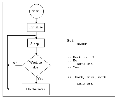
One of the best features of the PIC is its very low power consumption. This can be stretched to the maximum by using the SLEEP mode. To use this mode:
The watchdog timer must be enabled in the configuration word to use the watchdog as a wake up mechanism.
The prescaler divider (in the option register) can be assigned to the watchdog timer to stretch the time from 18 milliseconds to as long as 2.3 seconds.
Execute the SLEEP instruction.
When the PIC wakes up, it continues executing with the next instruction after the SLEEP. Examples of how this can be used are found in the LIGHTS.PIC and DSLOCKRC.PIC files.
The sleep mode does have various restrictions. If interrupts are enabled, then the PIC will wake whenever an interrupt occurs. The internal clock is disabled which means that the timer will not increment while in sleep mode, so timer interrupts will not occur. Also, for all oscillator types other than RC, the clock takes a while to stabilise so there might be a slight execution hiccup before the PIC can service the interrupt.
While sleeping, the PIC only draws about 50mA. Alkaline AA cells have a capacity over 2AH so, theoretically, a PIC hooked up with a three AA cells should be able to last for 40 000 hours (about four and a half years!). However there are likely to be other current drains in the circuit and the PIC will not be sleeping all the time. Still, for certain applications, you should be able to construct circuits in this manner that run for over two years.
Often microcontroller software needs to store boolean (true/false- yes/no) values. Most microcontrollers provide support for bit operations on data, making them more suitable for performing these boolean operations than general purpose microprocessors. The PIC microcontroller supports four special bit oriented instructions:
|
BCF bit_selector |
Clear the specified bit |
|
BSF bit_selector |
Sets the specified bit |
|
BTFSC bit_selector |
Skip next instruction if the bit_selector is clear (0) |
|
BTFSS bit_selector |
Skip next instruction if the bit_selector is set (1) |
A typical program will require many boolean variables. Rather than use a single byte per variable, they can easily be grouped together and allocated using the RB and EQU assembler directives as follows:
flag_byte rb ; allocate a byte to be used for bit flags
boolean_0 equ flag_byte.0
boolean_1 equ flag_byte.1
boolean_2 equ flag_byte.2
boolean_3 equ flag_byte.3
boolean_4 equ flag_byte.4
boolean_5 equ flag_byte.5
boolean_6 equ flag_byte.6
boolean_7 equ flag_byte.7
This allows eight boolean values to be stored in a single byte. All the flags can be simultaneously manipulated or tested by using the byte oriented instructions, otherwise individual bits can be manipulated or tested by using the bit oriented functions:
clrf flag_byte ; clears all flags to zero
bsf boolean_4 ; sets just boolean_4
This concept can also be used for assigning functions to port pins on the PIC. For example:
LED equ porta.0
relay equ porta.1
bsf led ; drive the LED pin high.
bcf relay ; turn off relay drive pin.
The PICs provide no conditional branching except for the simple skip instructions:
|
DECFSZ f,d |
Decrement f, skip next instruction if zero |
|
INCFSZ f,d |
Increment f, skip next instruction if zero |
|
BTFSC bit_selector |
Skip next instruction if the bit_selector is clear (0) |
|
BTFSS bit_selector |
Skip next instruction if the bit_selector is set (1) |
Assembler programmers familiar with other microcontrollers might expect a richer set of conditional branching. These can be emulated quite simply with the PIC instruction set.
Example: Jump to where if the value of what is zero.
MOVF what,f ; moves the value in what back to itself.
; This does nothing
except update the Zero flag
; Now the Zero flag will
be 1 if what was zero
BTFSC Zero ; skip next instruction if Zero flag is 0
GOTO where ; this instruction will be executed if the
; Zero flag is 1, ie if
what is zero
Example: Jump to where if the value in what is not equal to 5.
MOVLW 5 ; puts 5 in W register
XORWF what,w ; XORs what with w, putting result in w
; w will be zero and
the zero flag will be set
; if what is 5
BTFSS Zero ; skip if Zero flag is set
GOTO where ; this instruction will be executed if the
; zero flag was 0, ie
if what is not equal to 5
This section shows the implementation of a simple circuit which receives and transmits RS232 data in half-duplex mode. This basic code uses very little of the PIC's capability, allowing the circuit and the software to be extended quite easily. The code for this example is quite small (about 80 instructions in all), yet still illustrates quite a few concepts.
Note that this is by no means the most efficient RS232 handling code, but it has been structured to be readily understood, yet still reasonably efficient. This code is capable of receiving or transmitting data at a rate of up to 2400 baud with a 4MHz crystal.
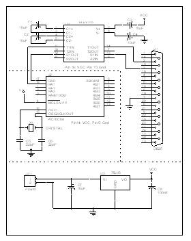
Circuit diagram
The circuit is extremely simple and is made up of three sections:
The PIC microcontroller and oscillator circuit. The circuit uses a crystal oscillator as it needs more accuracy than can be provided by an RC oscillator.
The power supply section to provide 5V DC.
The RS232 interface, comprising the MAX232 and associated capacitors and a standard RS232 connector.
This circuit leaves plenty of extra pins for extending the circuit.
Well if the hardware was so simple, where's the magic? You guessed it -- in the software.
This software receives characters with 8 data bits, 1 stop bit and no parity. Each RS232 character is transmitted as a start bit (0), the eight data bits starting with the least significant bit, and finally the stop bit (1), adding up to ten bits in total.
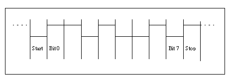
Of course the first problem when receiving is to sample the bits, but it is also important to sample somewhere near the middle of each bit since this is where the signal is cleanest. If we were to sample right near the edge of a bit, then a slight timing glitch could cause us to sample the wrong bit and thus give incorrect data. The way that this is achieved is to sample the signal as follows:
While waiting for the start bit, sample at three times the baud rate, or a third of a bit period between samples.
When the start bit is detected, wait one and a third bit periods before sampling data bit 0.
Wait for one bit period before sampling each other bit.
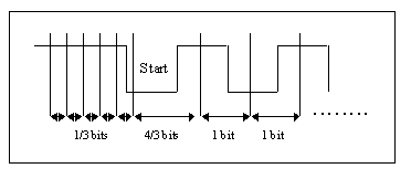
How does that all work? By sampling at three times the baud rate, we detect the start bit during the first third of the bit. By delaying four thirds of a bit period before sampling the first bit, we make sure that we sample the bit in the middle third of the bit. Subsequent bits are sampled in the middle third by waiting one bit period.
Receiving and transmitting RS232 is more a matter of precision timing than anything else. That's why a crystal was used instead of an RC oscillator. It is also a matter of waiting to perform the next sample, time that could be put to better use than hanging around waiting for the next sample time.
For these two reasons, we use a timer interrupt to provide the timing required to sample the RS232 signal. Other activity can progress in the main program while the RS232 communications is handled completely in the background by the timer interrupt service routine.
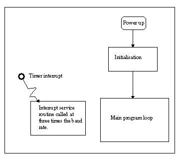
The structure of interrupt driven programs is very different to normal sequential programs. The main reason for this is that interrupts just run for a short while, then return. In main programs, it is easy to track where you are in an sequence of operations because the main program effectively is that sequence. In an interrupt driven program, you have to manually track that sequence; when the interrupt service routine starts up, it must first find out where it left off, then decides what to do based on its current state.
This isn't really as difficult as it sounds. You just need to work out the states on paper (that's called a State Diagram or State Table, depending on whether it's a picture or a table) before you write the program.
If you look at the serial receiving code you will see that it hinges around ten states in a variable called bitcnt, one state for each bit to be received. As each bit is received, the software proceeds to the next state. Notice here that the states count backwards from 9 to 0. Here's effectively what happens:
State 9: Waiting for start bit.
If a start bit is detected, then set next timer for 4/3 bit periods and set the
state to 8. Otherwise set the next timer for 1/3 bit periods and leave in state
9.
States 8..1: Waiting for data
bits.
Sample the data bit, set the next timer for one bit period and decrement the
sate. Note that after the last bit has been detected, the state will be zero.
State 0: Waiting to get into
stop bit area.
The RS232 signal is now in the stop bit area which means that it is safe to try
detecting the next start bit. A complete byte has been received, so the execution
is passed to rx_byte_complete for
further processing. At this stage sio_byte
contains the received byte.
The software to perform a transmit is similar but a bit simpler mainly because there is no need to perform start bit detection and each time interval is only one bit period long. When a transmit has completed, the execution is passed to tx_byte_complete
The software is highly modular which allows it to be extended very easily. The interface is defined by the following functions:
sio_init: Sets up the ports and timer and initialises the interrupts for serial communications.
rx_byte: This subroutine is executed to initiate a byte receive. When the byte has been received, then execution is passed to rx_byte_complete with the received byte in sio_byte
tx_byte: This subroutine is executed with the byte to be transmitted in sio_byte to initiate a byte transmit. When the byte has been received, then execution is passed to rx_byte_complete
The following code shows a very simple test rig for the serial communications module:
;; tx_byte_complete is executed when a byte has been transmitted
tx_byte_complete
goto rx_byte
;; rx_byte_complete is executed when a byte has been received
rx_byte_complete
incf sio_byte,f
goto tx_byte
;; Main program starts here
boot_up
call sio_init ; initialises the serial communications
call rx_byte ; readies the serial module to receive a byte
loop_forever
clrwdt
goto loop_forever
This code waits for a character. When it is received, then the character is incremented and sent back. For example if the PIC receives an 'a', then it sends back a 'b'.
How this works:
When the PIC starts up, it calls sio_init to initialise the serial module, then calls rx_byte to ready the communications module to receive the first byte. It then enters an infinite loop.
When a byte transmission is completed, the communications module jumps to tx_byte_complete which just executes rx_byte to ready the module to receive the next byte.
When a byte receive is completed, the communications module jumps to rx_byte_complete which increments the byte and executes tx_byte to transmit it.
Of course this isn't very useful as it stands, but it is quite straight forward to extend it to perform a real task.
This assembler is fully functional and I have not needed anything else even though it was constructed primarily as a learning tool. Once you've gained confidence with the PIC, you may feel the urge to step up to the "big league" and use a more powerful assembler (which has more to learn). If you do, I would strongly recommend using the assembler supplied by Microchip. This can be downloaded from their internet web page.
There are numerous information sources on internet.
Some WWW pages:
https://www.paranoia.com/~filipg/HTML/LINK/ELE/F_PIC_faq.html
https://www.ultranet.com/biz/mchip/
https://www.parallaxinc.com/
There is a PIC discussion list at MIT. To subscribe to this send an email to [email protected] with the following line in the body:
subscribe piclist <your name>
eg.
subscribe piclist John F. Smith
QUASAR ELECTRONICS
Unit 14 Sunningdale
BISHOP'S STORTFORD
Herts
CM23 2PA
EMAIL: [email protected]
WEBSITE: https://www.quasarelectronics.com/home.htm
TEL: +44 (0)1279 306504
FAX: +44 (0)870 7064222
|