Service Manual
PREMIUM-X 7000P
Version : 0.1
INDEX
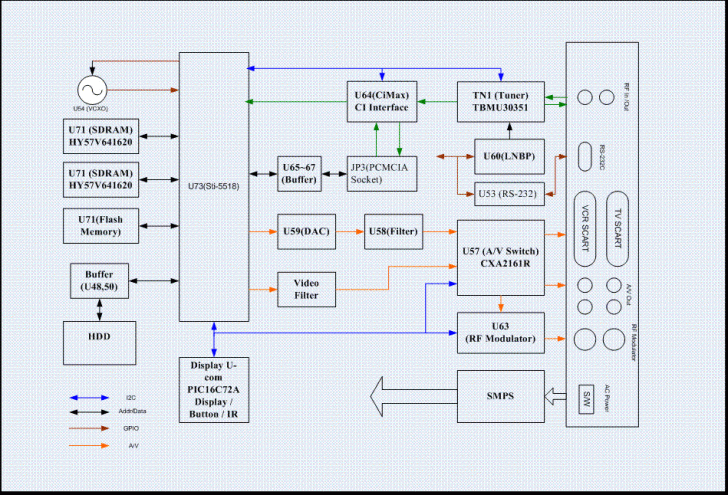
Wire connection3. Set Block Diagram
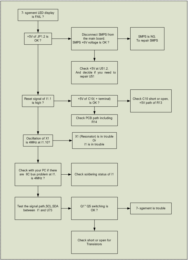
1) Front Panel display trouble
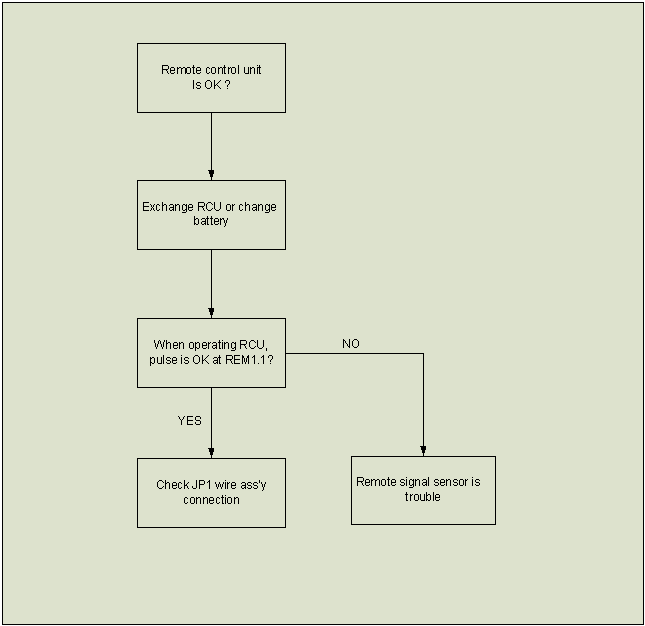
2) Remote control unit trouble
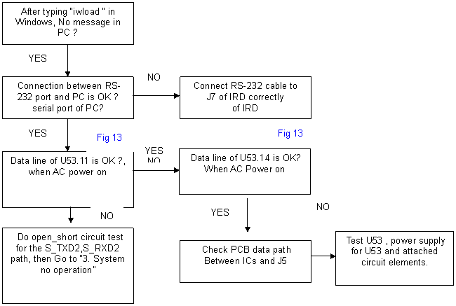
3) System no operation (¡° No message in PC monitoring by serial RS-232¡± )
8) Slow / Quick switching trouble
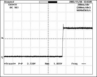
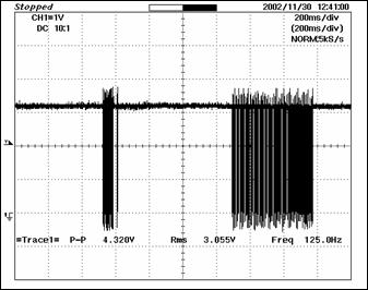
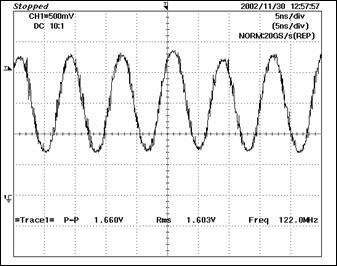
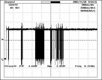
5. Waveforms of important point
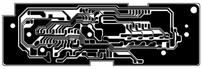
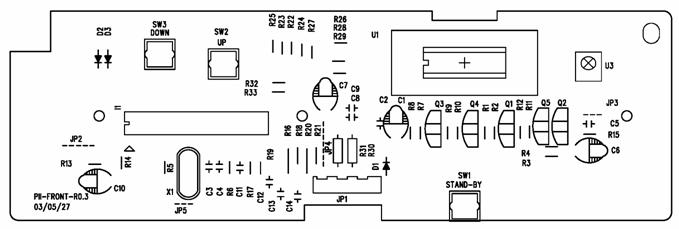
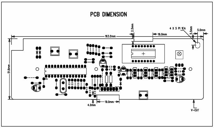
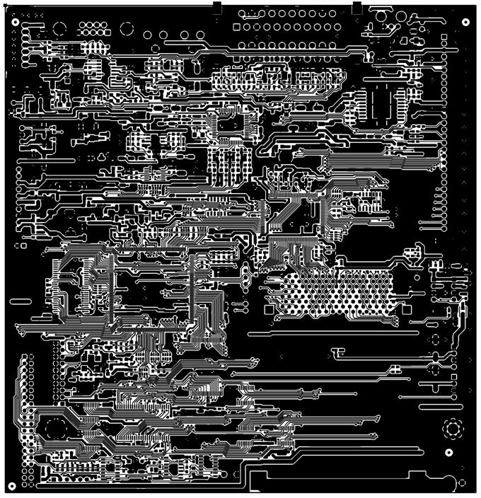
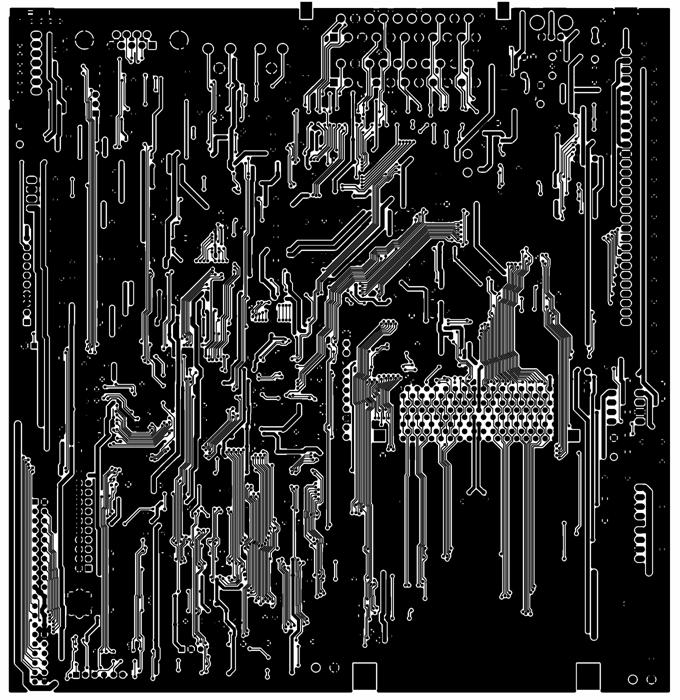
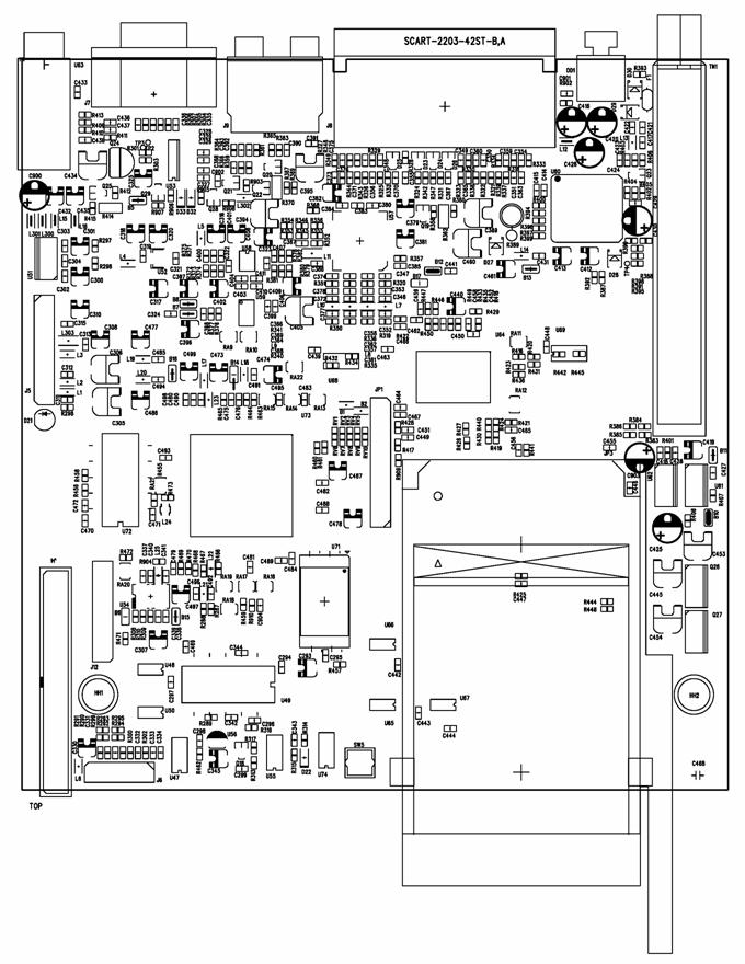
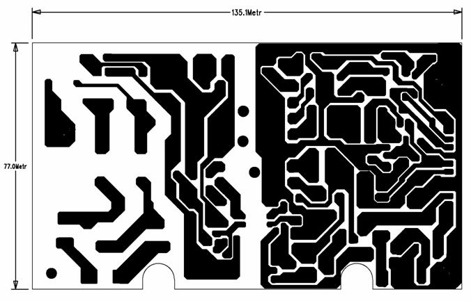
PCB Silk sheet & pattern
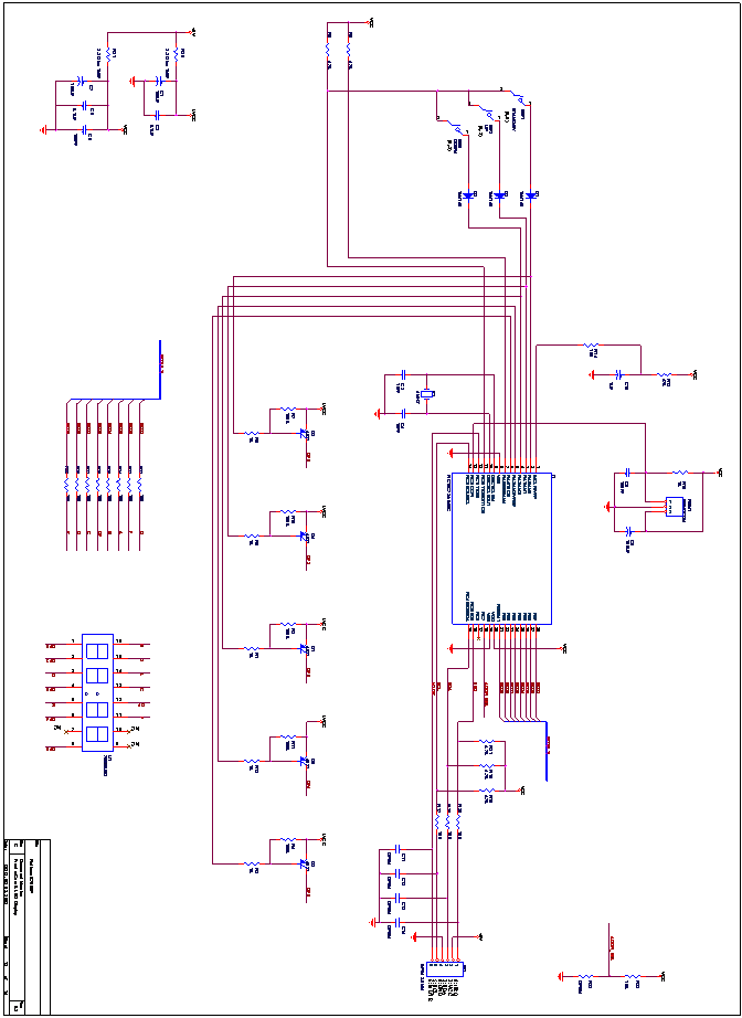
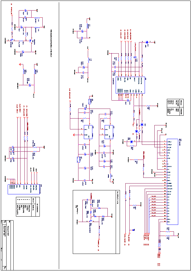
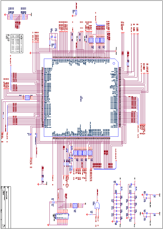
8. Document & Block Diagram of important IC
CIMAX
LNBP20 :
RMUP74055WL
21) 74LVT245 : 3.3V ABT OCTAL BUS TRANCEIVER WITH 3-STATE OUTPUTS
22) ST340015ACE : HARD DISC DRIVER / CE MODEL
Transmission Standards
DVB,MPEG2
LNB/Tuner input
Connector 2 x F-type
(Loop Through)
Input frequency 950-2150MHz
Max Current 400mA max
Supply Voltage 13V/18V
DiSEqC 1.2
RF Impedance 75 ohm
Demodulator
QPSK
Symbol rate 2-45Ms/s
SCPC and MCPC capable
Video decoder
MPEG-2 Main Profile @ Main Level
Data rates up to 15Mbit/s
Video formats
Audio decoder
MPEG-2 layer 1 & 2
Stereo, Mono, Dual channel, Joint stereo
System resources
Processor 80MHz
Shared Memory for MPEG
/CPU/Graphic 16Mbytes x 2
Flash ROM 2Mbytes
Resolution 720X576
OSD 256 colors
RF Modulator
Output Channel 21-69
Output Signal PAL B/G/I
Input/Output Connectors
IEC169-2 male/female
Preset Channel 43
TV SCART
RGB, CVBS, Audio
AUX SCART
CVBS, Audio
Audio Output
Hi-Fi RCA (Cinch) connector
S/PDIF optical output
Video Output
RCA (Cinch) connector
Serial Data
9pin D-sub RS232C signal
Baud rates 115.2Kbaud max
Remote Controller
Type NEC
Operating distance 10 meters
Batteries 2 x 1.5V AAA
Conditional Access System
No Embedded CAS
2 CI Interfaces (DVB Standard)
CAS Support with CI CAM ;
Irdeto, Viaccess, Nagravision, Astoncrypt ,
Alphacrypt and Cryptoworks
Hard Disc Driver
Formatted Gbyte : 40Gbytes
Interface Ultra ATA/66
Spindle Speed 5,400RPM
Rear Panel Interfaces
LNB IF IN/OUT
RF modulator IN/OUT
2 x SCART for TV and AUX
1 x RCA Audio (L/R, Cinch)
1 x RCA Video (CVBS, Cinch)
RS232C (9pin D-Sub)
Optical Digital Output
Power On/Off Switch
Power Connector
General Data
Operating Temperature 5 C to 45 C
Storage temperature -40 C to +70 C
Supply Voltage 90-250V ~AC / 50~60Hz
Power Consumption 35W Max
Dimension (WxDxH) : 340mmx240mmx65mm
Weight : 3.47Kg
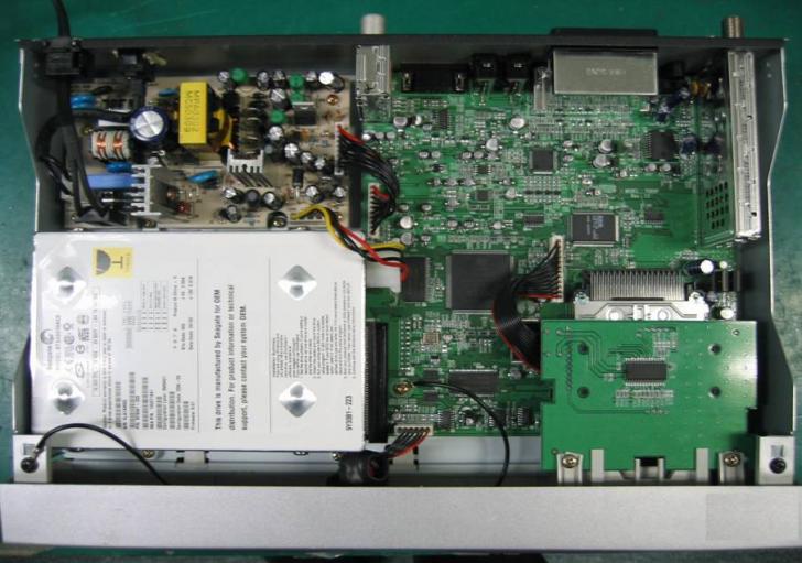 2. Wire connection
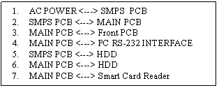
![]()
|
No problem
![]()

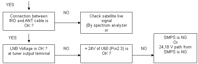
![]()
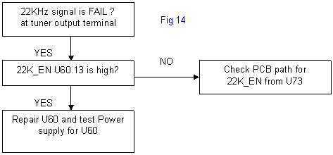
NO
![]()
Tuner
(TN1) is in trouble
TV Scart /
AUX Scart /C-inch
video is FAIL ?
Test Q19,Q22 Test PCB
path for the TV_CVBS_OUT,RCA_CVBS_OUT and VCR_YOUT,COUT U57 may
be in trouble, So
replace it -5V(Pin21),+5V(Pin24) is OK? Test the
Power path from SMPS Scart
cable or C-inch cable Connection
is OK ? Connect
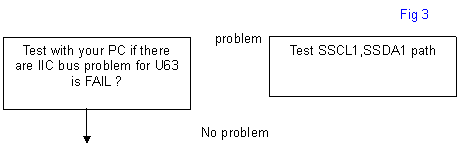
cables to TV correctly Test with your PC if there are IIC BUS problem about
U57: CXA2161R Do
open_short circuit test for SCL,SDA of U57 (Pin 35,34) Fig 15 Fig 3
![]()

![]()
![]()
![]()
![]()
Slow
switch +6 V is FAIL ? (16:9
mode) Slow
switch +12 V is FAIL ? (4:3 mode)
![]()
YES

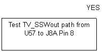
Test
TV_SSWout path from U57 to J8A Pin 8
![]()
TV Scart /
AUX Scart /C-inch audio
is FAIL ?
![]()
Fig 15 Do
open-short circuit test for SCL,SDA(Pin35,34) path Test the power path from SMPS U58 working is OK? YES Do Audio_left/right path test and repair U57 Repair U58 and test if
U59 working is OK. If needed, repair U59. Audio
output of U57(Pin 25,26 Pin27,28 Pin30,31) is OK ? Test
audio path from U57 to scart and RCA jack. Fig 3 Connect
cables to TV correctly Scart
cable or C-inch cable Connection
is OK ? Test with
your PC if there are IIC BUS problem about U57 +12V (Pin
15,U57) is OK?

![]()
![]()
![]()
![]()
![]()
![]()
![]()
![]()
![]()
![]()
10) RF modulator trouble
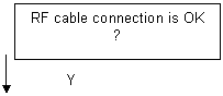
Connect RF
cable to TV correctly![]()
B+5V(Pin1),MB+5V(Pin4) And VT+30V
is OK?,U63 Test the
power path from SMPS.![]()
Y Fig
15 Test
Mod_VIDEO,AUDIO signal path. Test U63. If necessary,
replace U63
![]()
![]()
AUX to TV
bypass FAIL ?
![]()
+6V or
+12V of Scart connector J8B (Pin 29) is OK ?
Check AUX
cable to AUX Scart ![]()
![]()
Check PCB
path for VCR_ SSWIN Check
VCR_YCIN , VCRAUDIO_LIN,RIN path from scart to U67
![]()
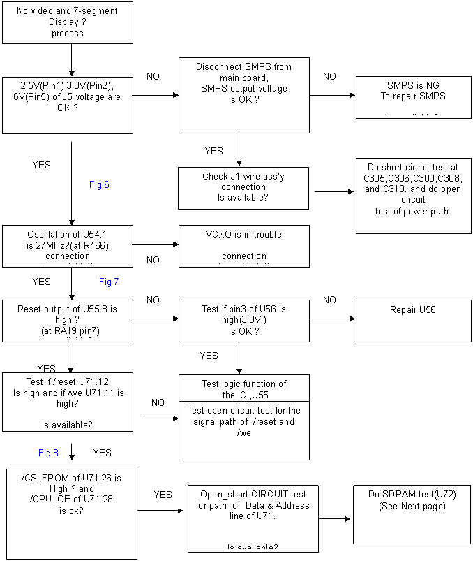
1.Fig 1 2.Fig
2
- Reset signal for front u-com working - 4MHz oscillation for Front u-com working
By power on, it¡¯s working as active ¡° Low¡±
3. Fig 3-1 4
Fig 3-2
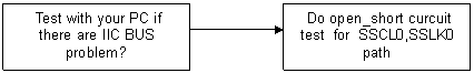
- IIC bus signal - IIC bus signal
SSCL0 & SSDA0 - SSCL1 & SSDA1
5. Fig 4
6. Fig 5
- Segment driving signal to display digit - Remocon pulse at sensor
Colletor voltage of terminal(Q1~Q5) - (Pin 1 of REM1)
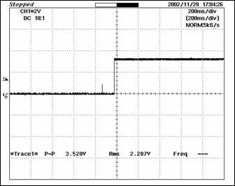
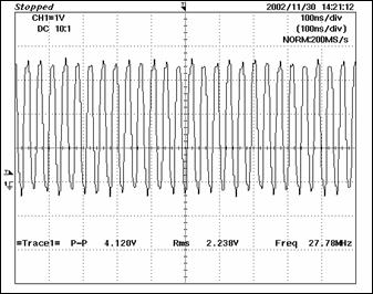
7. Fig 6 8. Fig 7
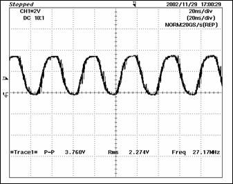
- 27MHz oscillation at VCXO for main - Reset input of U73(STi5518)
main system clock
9. Fig 8-1
10.
Fig 8-2
- Flash memory chip select signal - Flash memory write enable signal
/CS_FROM - CPU_R/W
11. Fig 8-3 12.
Fig 9
- Flash memory output enable signal - SDRAM clock signal
- /CPU_OE - SMI_CLK
13. Fig 10
14.
Fig 11-1
- SDRAM chip select signal - SDRAM RAS signal
SMI_CS0 - SMI_RAS
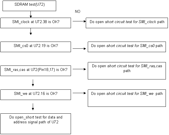
15 .Fig 11-2
16. Fig 12
- SDRAM CAS signal - SDRAM write enable signal
SMI_CAS SMI_WE
17. Fig 13-1 18.
Fig 13-2
- ST232 TX input signal - ST232 TX output signal
T1IN T1OUT
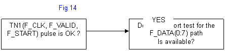
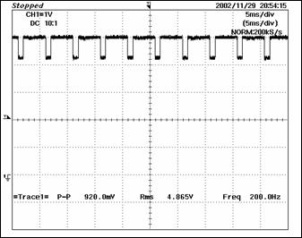
19. Fig 14-1 20. Fig 14-2
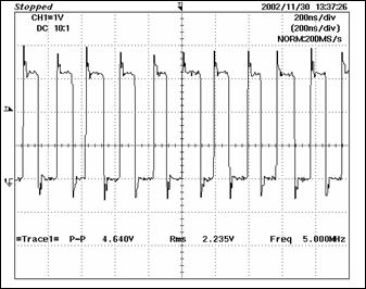
- TS clock signal from Tuner - TS valid from Tuner
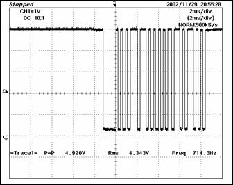
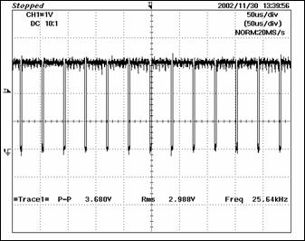
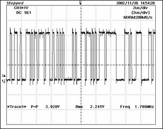
F_CLK F_VALID
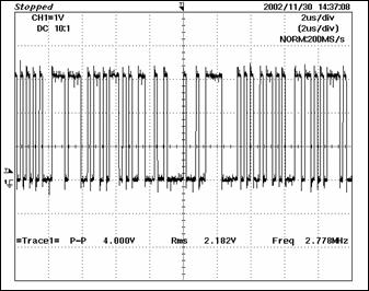
21. Fig 14-3 22. Fig14-4
- TS start signal from Tuner - 22KHz signal from Tuner
F_START - 22KHz
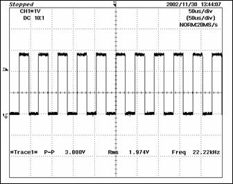
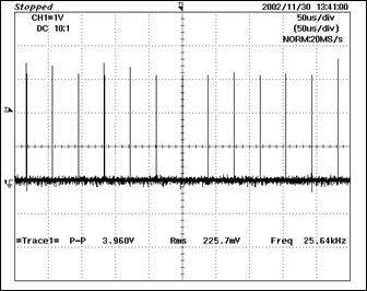
23. Fig 15-1
24. Fig 15-2
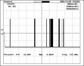
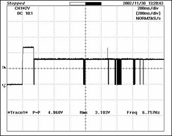
- CVBS signal for composite Video - Audio signal(L & R)
TV CVBS
25. Fig 16-1 26.Fig 16-2
- F-Data 0 - TS data 0
27. Fig 17
- 27MHz signal for CIMAX
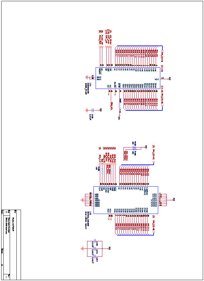
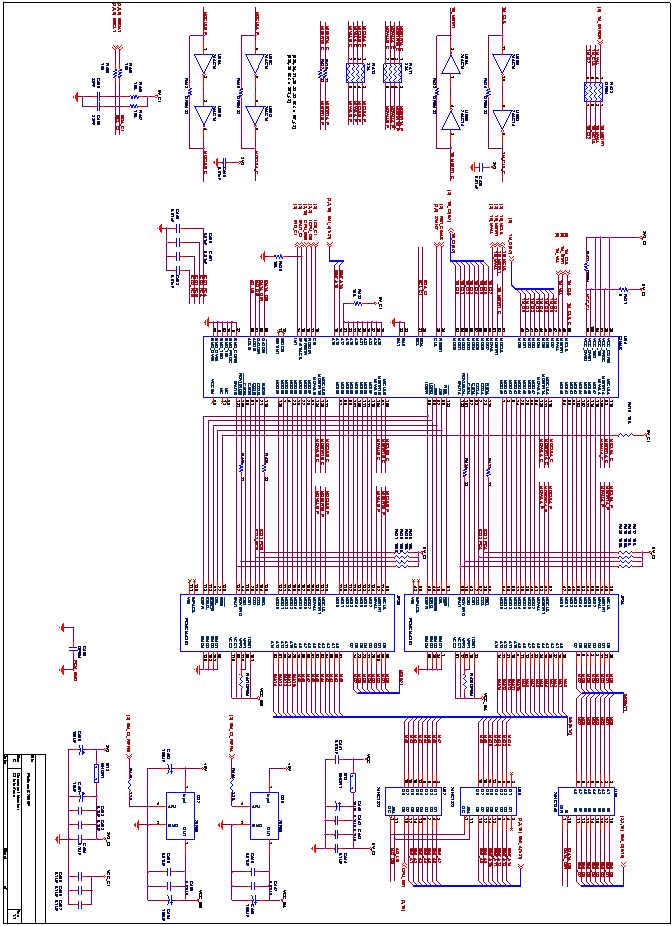
STi5518 : SINGLE-CHIP SET-TOP BOX DECODER
HY29LV160BT : 16MBIT(2M x 8/1M x 16) LOW VOLTAGE FLASH MEMORY
HY57V651620B : 4BANKS x 1M x 16BIT SYNCHRONOUS DRAM
CIMAX : DUAL COMMON INTERFACE HARDWARE CONTROLLER
LNBP20 : LNBP SUPPLY AND CONTROL VOLTAGE REGULATOR
UDA1330 : LOW COST STEREO FILTER DAC
CXA2161R : A/V SWITCH AND ELECTRONIC VOLUME CONTROL
ST232 : MULTI-CHANNEL RS-232 DRIVERS AND RECEIVERS
PIC16C72A : 8-BIT CMOS MICROCONTROLLERS WITH AD CONVERTER
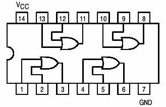
74AC14 : HEX INVERTER SCHMITT TRIGGER
74AC32 : QUAD 2-INPUT OR GATE
74HCT245 : OCTAL BUS TRANSCEIVER
74HCT373 : OCTAL D-TYPE TRANSPARENT LATCH
KA4558 : DUAL OPERATIONAL AMPLIFIER
KA78R05 : LOW DROPOUT VOLTAGE REGULATOR
KA7805 : 3 TERMINAL 1A POSIIVE VOLTAGE REGULATOR
KA79L05 : 3 TERMINAL 0.1A NEGATIVE VOLTAGE REGULATOR
KA75270 : VOLTAGE DETECTOR
TBMU30351PB : DIGITAL CHANNEL MODULE
RMUP74055WL : RF MODULATOR
74LVT245 : 3.3V ABT OCTAL BUS TRANCEIVER WITH 3-STATE OUTPUTS
ST340015ACE : HARD DISC DRIVER / CE MODEL
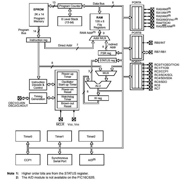
1) STi5518
SINGLE-CHIP SET-TOP BOX DECODER
DESCRIPTIONS
The STi5518 is a highly integrated single-chip decoder, designed for use in feature-rich mass-market set-top boxes. It integrates a high-performance 32-bit CPU, a dedicated block for DVB/DirecTV transport demultiplexing and descrambling, modules for MPEG-2 video and audio decoding with 3D-surround and MP3 support, advanced display and graphics features, a digital video encoder and all of the system peripherals required in a typical low-cost interactive receiver.
To cover the needs of DVD-capable set-top boxes, STi5518 integration options include a CSS decryption block, a Dolby Digital audio decoder and Macrovision copy protection.
An ATAPI interface is built-in, supporting the glueless connection of standard Hard Disk Drives. In this way, the STi5518 is ideal for set-top boxes featuring trick modes such as live TV recording, pausing and time-shifting. The STi5518 is backward compatible with the popular STi5500 set-top box decoder, allowing easy migration from the previous generation.
FEATURES
Integrated 32-bit host CPU up to 81 MHz
- 2 Kbytes of Icache, 2 Kbytes of Dcache, and 4 Kbytes of SRAM configurable as Dcache.
Audio decoder
- 5.1 channel Dolby Digital¢ç /MPEG-2 multi-channel decoding, 3 X 2-channel PCM outputs
- IEC60958 -IEC61937 digital output
- SRS¢ç/TruSurround¢ç
- DTS¢ç digital out and MP3 decoding
- Alignment beep for satellite dishes.
Video decoder
- Supports MPEG-2 MP@ML
- Fully programmable zoom-in and zoom-out
- NTSC to PAL conversion.
DVD and SVCD subpicture decoder
High performance on-screen display
-
- Anti-flicker, anti-flutter and anti-aliasing filters.
PAL/NTSC/SECAM encoder
- RGB, CVBS, Y/C and YUV outputs with 10-bit DACs
- Macrovision¢ç 7.01/6.1 compatible (optional).
Shared SDRAM memory interface
- 1 or 2x16-Mbit, or 1x64-Mbit 125 MHZ SDRAM.
Programmable CPU memory interface for SDRAM, ROM, peripherals...
Front-end interface
- DVD, VCD, SVCD and CD-DA compatible
- Serial, parallel and ATAPI interfaces
- Hardware sector filtering
- Integrated CSS decryption and track buffer.
Hardware transport-stream demultiplexor
- Parallel/serial input
- DES and DVB descramblers
- 32 PID support.
Integrated peripherals
- 2 UARTs, 2 SmartCards, I C controller, 3 PWM outputs, 3 capture timers
- Modem support
- 44 bits of programmable I/O
- IR transmitter/receiver.
Professional toolset support
- ANSI C compiler and libraries.
208 pin PQFP package.
BLOCK DIAGRAM
16MBIT(2M x 8/1M x 16) LOW VOLTAGE FLASH MEMORY
FEATURES
Single Power Supply Operation
- Read, program and erase operations from 2.7 to 3.6 volts deal for battery-powered applications
High Performance
- 70, 80, 90 and 120 ns access time versions
Ultra-low Power Consumption (Typical Values At 5 Mhz)
- Automatic sleep mode current: 1 µA
- Standby mode current: 1 µA
- Read current: 9 mA
- Program/erase current: 20 mA
Flexible Sector Architecture:
- One 16 KB, two 8 KB, one 32 KB and thirty-one 64 KB sectors in byte mode
- One 8 KW, two 4 KW, one 16 KW and thirty-one 32 KW sectors in word mode
- Top or bottom boot block configurations available
Sector Protection
- Allows locking of a sector or sectors to prevent program or erase operations
within that sector
- Sectors lockable in-system or via programming equipment
- Temporary Sector Unprotect allows changes in locked sectors
(requires high voltage on RESET# pin)
Fast Program and Erase Times
- Sector erase time: 0.25 sec typical for each sector
- Chip erase time: 8 sec typical
- Byte program time: 9 s typical
Unlock Bypass Program Command
- Reduces programming time when issuing multiple program command sequences
Automatic Erase Algorithm Preprograms and Erases Any Combination of Sectors or the Entire Chip
Erase Suspend/Erase Resume
- Suspends an erase operation to allow reading data from, or programming data to, a
sector that is not being erased
- Erase Resume can then be invoked to complete suspended erasure
Automatic Program Algorithm Writes and Verifies Data at Specified Addresses
100,000 Write Cycles per Sector Minimum
Data# Polling and Toggle Bits
- Provide software confirmation of completion of program and erase operations
Ready/Busy# Pin
- Provides hardware confirmation of completion of program and erase operations
Hardware Reset Pin (RESET#) Resets the Device to Reading Array Data
Compliant With Common Flash Memory Interface (CFI) Specification
- Flash device parameters stored directly on the device
- Allows software driver to identify and use a variety of different current and future
Flash products
Compatible With JEDEC standards
- Pinout and software compatible with single-power supply Flash devices
-
Space Efficient Packaging
- 48-pin TSOP and 48-ball FBGA packages
BLOCK DIAGRAM
PIN DESCRIPTION
|
Name |
Type |
Description |
|
A[ |
Inputs |
Address, Active High. These 20 inputs, combined with the DQ[15]/a[-1] input in Byte mode, select one location within the array for read or write operations |
|
DQ[15]/A[-1] DQ[ |
Inputs/Outputs Tri-state |
Data Bus, active High. These pins provide 8- or 16-bit data path for
read and write operations. In Byte mode, DQ[15]/A[-1] is used as the LSB of
the 21-bit byte address input. DQ[ |
|
BYTE# |
Input |
Byte mode, active low. Low selects Byte mode. High selects Word mode. |
|
CE# |
Input |
Chip Enable, active Low. This pin must be asserted to read data from or write data to the HY29LV160. When High, the data bus is tri-stated and the device is placed in the Standby mode. |
|
OE# |
Input |
Output Enable, active Low. Asserted for read operations and negated for write operations. BYTE# determines whether a byte or word is read during the read operation. |
|
WE# |
Input |
Write Enable, active Low. Controls writing of commands or command sequences in order to program data or erase sectors of the memory array. A write operation takes place when WE# is asserted while CE# is Low and OE# is high. |
|
RESET# |
Input |
Hardware Reset, active Low. Provides a hardware method of resetting the HY29LV160 to the read array state. When the device is reset, it immediately terminates any operation in progress. While RESET# is asserted, the device will be in the Standby mode. |
|
RY/BY# |
Output Open Drain |
Ready/Busy Status. Indicates whether a write or erase command is in progress or has been completed. Remains Low while the device is actively programming data or erasing, and goes High when it is ready to read array data. |
|
VCC |
|
3-volt (nominal) power supply. |
|
VSS |
|
Power and signal ground. |
4BANKS x 1M x 16BIT SYNCHRONOUS DRAM
FEATURES
Single 3.3+/-0.3V power supply Note)
All device pins are compatible with LVTTL interface
JEDEC standard 400mil 54pin TSOP-II with 0.8mm of pin pitch
All inputs and outputs referenced to positive edge of system clock
Data mask function by UDQM or LDQM
Internal four banks operation
Auto refresh and self refresh
4096 refresh cycles / 64ms
Programmable Burst Length and Burst Type
- 1, 2, 4, 8 or Full page for Sequential Burst
- 1, 2, 4 or 8 for Interleave Burst
Programmable CAS Latency ; 2, 3 Clocks
BLOCK DIAGRAM
PIN DESCRIPTION
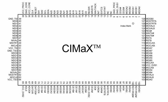
DUAL COMMON INTERFACE HARDWARE CONTROLLER
DESCRIPTION
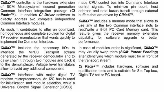
FEATURES
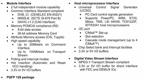
BLOCK DIAGRAM
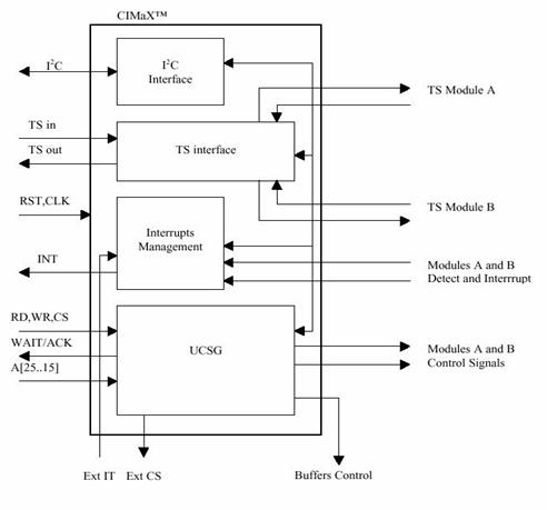
PIN DESCRIPTION
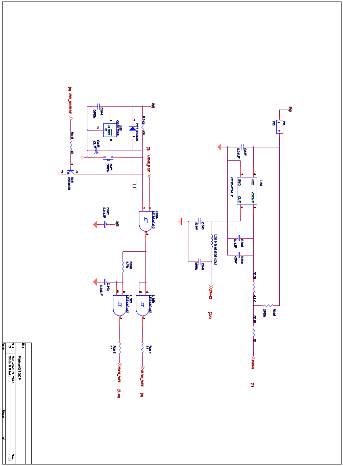
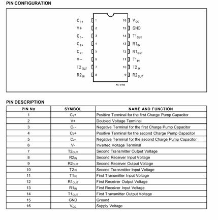
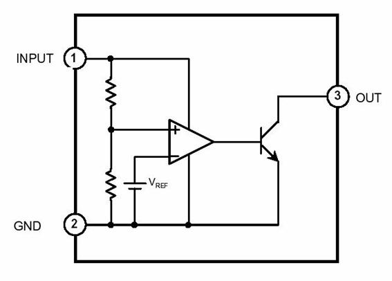
LNBP SUPPLY AND CONTROL VOLTAGE REGULATOR
FEATURES
Complete interface for two LNBs remote supply and control
LNB selection and stand-by function
Built-in tone oscillator factory trimmed at 22KHz
Fast oscillator start-up facilitates DiSEqC encoding
Two supply inputs for lowest dissipation
Bypass function for slave operation
LNB short circuit protection and diagnostic
Auxiliary modulation input extends flexibility
Cable length compensation
Internal over temperature protection
Backward current protection
BLOCK DIAFRAM
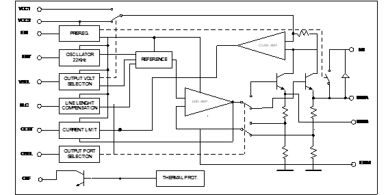
PIN DESCRIPTION
|
Symbol |
Name |
Function |
Pin No. |
|
VCC1 |
Supply Input1 |
15V to 25V supply. It is automatically selected when VOUT=13 or 14V |
|
|
VCC2 |
Supply Input2 |
22V to 25V supply. It is automatically selected when VOUT=18 or 19V |
|
|
LNBA |
|
In the stand-by mode this port is powered by the MI pin via the internal Bypass Switch |
|
|
VSEL |
Output Voltage Selection (13V or 18V) |
Logic Control Input |
|
|
EN |
Port Enable |
Logic Control Input |
|
|
OSEL |
Port Selection |
Logic Control Input |
|
|
GND |
Ground |
Circuit Ground |
|
|
ENT |
22KHz Tone Enable |
Logic Control Input |
|
|
CEXT |
External Capacitor |
Timing Capacitor used by the Dynamic Overload protection. Typical application is 4.7uF for a 1200ms cycle |
|
|
EXTM |
External Modulator |
External modulation input. Needs DC decoupling to the AC source, if not used, can be left open. |
|
|
LLC |
Line Length Compensation |
Logic Control Input |
|
|
OLF |
Over Load Flag |
Logic output(open collector). Normally in HIGH Impedance goes LOW when current or thermal overload occurs. |
|
|
MI |
Master Input |
In stand-by mode, the voltage on MI is routed to LNBA pin. Can be left open if bypass function is not needed |
|
|
LNBB |
|
|
|
LOW COST STEREO FILTER DAC
GENERAL DESCRIPTION
The UDA1330ATS is a single-chip stereo DAC employing bitstream conversion techniques.
The UDA1330ATS supports the I S-bus data format with word lengths of up to 20 bits, the MSB-justified data format with word lengths of up to 20 bits and the LSB-justified serial data format with word lengths of 16, 18 and 20 bits.
The UDA1330ATS can be used in two modes: L3 mode or the static pin mode.
In the L3 mode, all digital sound processing features must be controlled via the L3 interface, including the selection of the system clock setting.
In the two static modes, the UDA1330ATS can be operated in the 256fs and 384fs system clock mode.
Muting, de-emphasis for 44.1 kHz and four digital input formats (I S-bus or LSB-justified 16, 18, and 20 bits) can be selected via static pins. The L3 interface cannot be used in this application mode, so volume control is not available in this mode.
FEATURES
General
Low power consumption
Power supply voltage from 2.7 to 5.5 V
Selectable control via L3 microcontroller interface or via static pin control
System clock frequencies of 256fs fs and 512fs selectable via L3 interface or 256fs and 384fs via static pin
control
Supports sampling frequencies (fs ) from 8 to 55 kHz
Integrated digital filter plus non inverting Digital-to-Analog Converter (DAC)
No analog post filtering required for DAC
Slave mode only applications
Easy application
Small package size (SSOP16)
TTL tolerant input pads
Pin and function compatible with the UDA1320ATS.
Multiple format input interface
L3 mode: I S-bus, MSB-justified or LSB-justified 16, 18 and 20 bits format compatible
Static pin mode: I S-bus and LSB-justified 16, 18 and 20 bits format compatible
fs input format data rate.
DAC digital sound processing
Digital logarithmic volume control in L3 mode
Digital de-emphasis for 32, 44.1 and 48 kHz sampling frequencies in L3 mode or 44.1 kHz sampling frequency
in static pin mode
Soft mute control both in static pin mode and L3 mode.
Advanced audio configuration
Stereo line output (volume control in L3 mode)
High linearity, wide dynamic range and low distortion.
BLOCK DIAGRAM
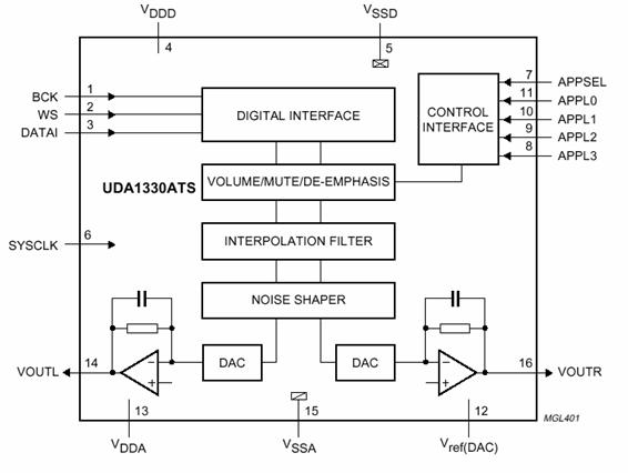
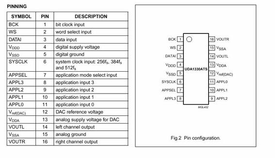
PIN DESCRIPTION
A/V SWITCH AND ELECTRONIC VOLUME CONTROL
DESCRIPTION
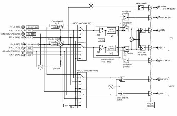
The Sony CXA2161R is an Audio/Video switch designed primarily for application in Digital Set Top Boxes. It provides video and audio routing from the digital encoder source to the TV and VCR scart (peri-television) connectors. In addition, the TV audio output has a programmable volume control. The chip is programmed by means of an I C interface and can operate from a single or dual power supply.
Target specifications: Canal+, BSkyB, TPS, NorDig, and ECCA Euro-Box
FEATURES
Supply
Single: 0V, +5V, +12V
Dual: 0V, –5V, +5V and +12V(Low number of external parts required)
Video
2 scart switching (VCR, TV)
VCR input supports RGB mode
Integrated 7drivers for direct video connection
Y/C mixer with trap for RF modulators
Switchable clamps on inputs
Adjustable gain on RGB outputs
Video output shutdown for low power modes
Fast blanking switch
Slow blanking switch for TV and VCR output
SVHS switch on VCR output
Y/C auxiliary input
Audio
Four stereo audio inputs
Volume control (–56dB to +6dB in 2dB steps)
Additional switchable gain on audio DAC inputs
Audio overlay facility
Volume bypass for TV and Phono outputs
Mono switching on TV, VCR outputs
High drive capability (60loads possible)
Switchable audio limiter function
Switchable Mono output for RF modulators
Audio output disable
I C and Logic
Fast mode compatible I C bus
Function monitor with loop through
Interrupt output for function monitor
Logic output pin
Sync detector for Y/CVBS inputs
BLOCK DIAGRAM
VIDEO and DIGITAL SECTION
AUDIO SECTION
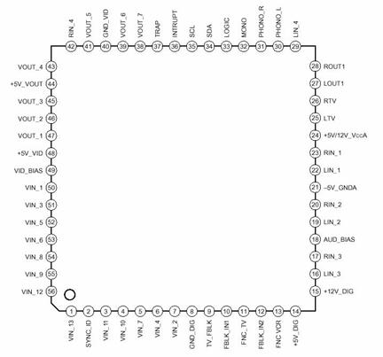
PIN DESCRIPTION
|
Pin No. |
Symbol |
Pin Voltage(V) |
Description |
|
|
|
VIN_1 VIN_2 VIN_4 |
|
RGB signal inputs |
|
|
|
VIN_3 |
|
RGB signal input or CVBS/Luminance signal input |
|
|
|
||||
|
|
VIN_5 VIN_7 |
|
RGB signal inputs or Chrominance signal inputs |
|
|
|
||||
|
|
VIN_6 VIN_13 |
|
Chrominance signal inputs |
|
|
|
VIN_8 VIN_9 VIN_10 VIN_11 VIN_12 |
|
CVBS/Luminance signal inputs |
|
|
|
VOUT_1 VOUT_2 VOUT_3 VOUT_4 VOUT_6 |
|
RGB signal outputs |
|
|
|
VOUT_5 |
|
Chrominance signal output |
|
|
|
VOUT_7 |
|
Typically RF modulator signal output (Minimum load resistance = 20Kohm) |
|
|
|
VID_BIAS |
|
Internal reference bias for video circuits. A capacitor is connected from this pin to GND Typically 100nF |
|
|
|
TRAP |
|
Connects trap circuit for subcarrier |
|
|
|
SYNC_ID |
|
Sync detect circuit time constant, resistor and capacitor Connection pin |
|
|
|
FBLK_IN1 FBLK_IN2 |
|
Fast blanking signal inputs |
|
|
|
TV_FBLK |
|
Fast blanking signal outputs |
|
|
|
FNC_VCR |
|
SCART function pin8 input/output to VCR |
|
|
|
FNC_TV |
|
SCART function pin8 output to TV |
|
|
|
LIN_1 RIN_1 LIN_2 RIN_2 LIN_3 RIN_3 LIN_4 RIN_4 |
(Single) |
Audio signal inputs |
|
|
(Dual) |
||||
|
|
LTV RTV LOUT1 ROUT1 PHONO_L PHONO_R MONO |
(Single) |
Audio signal outputs |
|
|
(Dual) |
||||
|
|
AUD_BIAS |
|
Internal reference bias for audio circuits |
Capacitor connected to GND(Typically 22uF) |
|
Connected directly to GND |
||||
|
|
LOGIC INTRUPT |
|
Open collector logic outputs Typically connect to +5V through 10Kohm resistor |
|
|
|
SCL |
|
I2C bus clock line |
|
|
|
SDA |
|
I2C bus data line |
|
|
|
+5V_DIG |
|
Digital supply |
|
|
|
+5V_VOUT |
Video output supply |
||
|
|
+5V_VID |
Video supply |
||
|
|
+12V_DIG |
|
Digital supply |
|
|
|
-5V_GNDA |
-5.0(Dual) 0.0(Single) |
Audio supply or Audio ground |
|
|
|
+5V/ +12V_VCCA |
5.0(Dual) 12.0(Single) |
Audio supply |
|
|
|
GND_DIG |
|
Digital ground |
|
|
|
GND_VID |
|
Video ground |
|
MULTI-CHANNEL RS-232 DRIVERS AND RECEIVERS
DESCRIPTION
The ST232 is a 2 driver, 2 receiver device following EIA/TIA-232 and V.28 communication standard. It is particularly suitable for applications where ¡¾12V is not available. The ST232 uses a single 5V power supply and only four external capacitors (0.mF). Typical applications are in:
Portable
Computers, Low Power Modems, Interfaces Translation,
FEATURES
SUPPLYVOLTAGERANGE: 4.5 TO5.5V
SUPPLYCURRENT NOLOAD(TYP): 5mA
TRANSMITTEROUTPUT VOLTAGESWING(TYP): ¡¾7.8V
ONTROLLEDOUTPUT SLEWRATE
RECEIVERINPUT VOLTAGERANGE:¡¾30V
DATA RATE(TYP): 220Kbps
OPERATINGTEMPERATURE RANGE: -40 TO85 o C, 0 TO70 o C
COMPATIBLEWITH MAX232 ANDMAX202
PIN DESCRIPTION
8-BIT CMOS MICROCONTROLLERS WITH AD CONVERTER
FEATURES
• High-performance RISC CPU
• Only 35 single word instructions to learn
• All single cycle instructions except for program branches, which are two cycle
• Operating speed: DC - 20 MHz clock input
DC - 200 ns instruction cycle
• 2K x 14 words of Program Memory, 128 x 8 bytes of Data Memory (RAM)
• Interrupt capability
• Eight level deep hardware stack
• Direct, indirect, and relative addressing modes
• Power-on Reset (POR)
• Power-up Timer (PWRT) and Oscillator Start-up Timer (OST)
• Watchdog Timer (WDT) with its own on-chip RC oscillator for reliable operation
• Brown-out detection circuitry for Brown-out Reset (BOR)
• Programmable code-protection
• Power saving SLEEP mode
• Selectable oscillator options
• Low-power, high-speed CMOS EPROM technology
• Fully static design
• In-Circuit Serial Programmin(ICSP)
• Wide operating voltage range: 2.5V to 5.5V
• High Sink/Source Current 25/25 mA
• Commercial, Industrial and Extended temperature ranges
• Low-power consumption:
- < 2 mA @ 5V, 4 MHz
- 22.5 mA typical @ 3V, 32 kHz
-< 1 mA typical standby current
• Timer0: 8-bit timer/counter with 8-bit prescaler
• Timer1: 16-bit timer/counter with prescaler, can be incre-mented during sleep via external crystal/clock
• Timer2: 8-bit timer/counter with 8-bit period register, pre-scaler and postscaler
• Capture, Compare, PWM module
• Capture is 16-bit, max. resolution is 12.5 ns, Compare is 16-bit, max. resolution is 200 ns, PWM maximum resolution is 10-bit
• 8-bit multi-channel Analog-to-Digital converter
•
Synchronous
SPI and I C
BLOCK DIAGRAM
PIN DESCRIPTION
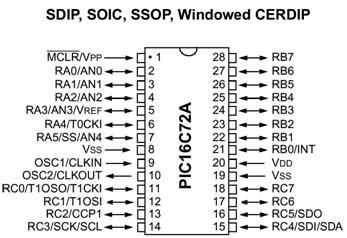
|
Pin Name DIP SOIC I/O/P Buffer Description PIN# PIN# TYPE TYPE |
|
OSC1/CLKIN 9 9 I ST/CMOS (3) Oscillator crystal input/external clock source input. |
|
OSC2/CLFAILUT 10 10 O - Oscillator crystal output. Connects to crystal or resonator in crystal oscillator mode. In RC mode, the OSC2 pin outputs CLFAILUT which has 1/4 the frequency of OSC1, and denotes the instruction cycle rate. |
|
MCLR/VPP 1 1 I/P ST Master clear (reset) input or programming voltage input. This pin is an active low reset to the device. |
|
PORTA is a bi-directional I/O port. RA0/AN0 (4) 2 I/O TTL RA0 can also be analog input 0 RA1/AN1 (4) 3 I/O TTL RA1 can also be analog input 1 RA2/AN2 4 I/O TTL RA2 can also be analog input 2 RA3/AN3/VREF (4) 5 I/O TTL RA3 can also be analog input 3 or analog reference voltage RA4/T0CKI Output is open drain type. RA5/SS/AN4 7 I/O TTL RA5 can also be analog input 4 or the slave select for the synchronous serial port. |
|
PORTB is a bi-directional I/O port. PORTB can be software programmed for internal weak pull-up on all inputs. RB0/INT 21 21 I/O TTL/ST (1) RB0 can also be the external interrupt pin. RB1 22 22 I/O TTL RB2 23 23 I/O TTL RB3 24 24 I/O TTL RB4 25 25 I/O TTL Interrupt on change pin. RB5 26 26 I/O TTL Interrupt on change pin. RB6 27 27 I/O TTL/ST (2) Interrupt on change pin. Serial programming clock. RB7 28 28 I/O TTL/ST (2) Interrupt on change pin. Serial programming data. |
|
PORTC is a bi-directional I/O port. RC0/T1OSO/T1CKI 11 11 I/O ST RC0 can also be the Timer1 oscillator output or Timer1 clock input. RC1/T1OSI RC2/CCP1 output/PWM1 output. RC3/SCK/SCL for both SPI and I C modes. RC4/SDI/SDA (I2 C mode). RC5/SDO RC6 RC7 |
|
VSS 8, 19 8, 19 P — Ground reference for logic and I/O pins. |
|
VDD 20 20 P — Positive supply for logic and I/O pins. |
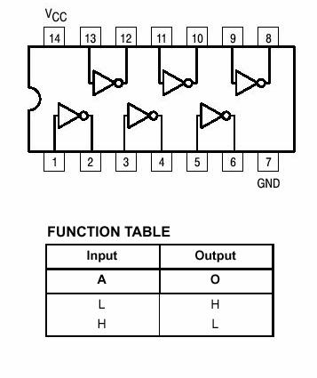
HEX INVERTER SCHMITT TRIGGER
DESCRIPTION
The MC74AC14/74ACT14 contains six logic inverters which accept standard CMOS Input signals (TTL levels for MC74ACT14) and provide standard CMOS output levels. They are capable of transforming slowly changing input signals into sharply defined, jitter–free output signals. In addition, they have a greater noise margin then conventional inverters. The MC74AC14/74ACT14 has hysteresis between the
positive–going and negative–going input thresholds (typically 1.0 V) which is determined internally by transistor ratios and is essentially insensitive to temperature and supply voltage variations.
Schmitt Trigger Inputs
Outputs Source/Sink 24 mA
4ACT14 Has TTL Compatible Inputs
QUAD 2-INPUT OR GATE
FEATURES
Outputs Source/Sink 24 mA
ACT32 Has TTL Compatible Inputs
PIN DESCRIPTION
OCTAL BUS TRANSCEIVER
DESCRIPTION
The 74HC/HCT245 are high-speed Si-gate CMOS devices and are pin compatible with low power Schottky TTL (LSTTL). They are specified in compliance with JEDEC standard no. 7A.
The 74HC/HCT245 are octal transceivers featuring non-inverting 3-state bus compatible outputs in both send and receive directions. The ¡°245¡± features an output enable (OE) input for easy cascading and a send/receive (DIR) for direction control. OE controls the outputs so that the buses are effectively isolated. The ¡°245¡± is similar to the ¡°640¡± but has true (non-inverting) outputs.
FEATURES
Octal bidirectional bus interface
Non-inverting 3-state outputs
Output capability: bus driver
ICC category: MSI
PIN DESCRIPTION
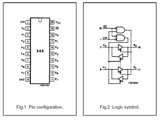
|
PIN NO. |
SYMBOL |
NAME AND FUNCTION |
|
|
DIR |
direction control |
|
|
A to A |
data inputs/outputs |
|
|
GND |
ground (0 V) |
|
|
B to B |
data inputs/outputs |
|
|
OE |
output enable input (active LOW) |
|
|
VCC |
positive supply voltage |
OCTAL D-TYPE TRANSPARENT LATCH
DESCRIPTION
The 74HC/HCT373 are high-speed Si-gate CMOS devices and are pin compatible with low power Schottky TTL (LSTTL). They are specified in compliance with JEDEC standard no. 7A. The 74HC/HCT373 are octal D-type transparent latches featuring separate D-type inputs for each latch and 3-state outputs for bus oriented applications. A latch enable (LE) input and an output enable (OE) input are common to all latches.
The ¡°373¡± consists of eight D-type transparent latches with 3-state true outputs. When LE is HIGH, data at the Dn inputs enters the latches. In this condition the latches are transparent, i.e. a latch output will change state each time its corresponding D-input changes. When LE is LOW the latches store the information that was present at the D-inputs a set-up time preceding the HIGH-to-LOW transition of LE. When OE is LOW, the contents of the 8 latches are available at the outputs.
When OE is HIGH, the outputs go to the high impedance OFF-state. Operation of the OE input does not affect the state of the latches.
The ¡°373¡± is functionally identical to the ¡°533¡±, ¡°563¡± and ¡°573¡±, but the ¡°563¡± and ¡°533¡± have inverted outputs and the ¡°563¡± and ¡°573¡± have a different pin arrangement.
FEATURES
3-state non-inverting outputs for bus oriented applications
Common 3-state output enable input
Functionally identical to the ¡°563¡±, ¡°573¡± and ¡°533¡±
Output capability: bus driver
ICC category: MSI
PIN DESCRIPTION
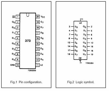
|
PIN NO. |
SYMBOL |
NAME AND FUNCTION |
|
|
OE |
3-state output enable input (active LOW) |
|
|
Q to Q |
3-state latch outputs |
|
|
GND |
ground (0 V) |
|
|
D to D |
data inputs |
|
|
LE |
latch enable input (active HIGH) |
|
|
VCC |
positive supply voltage |
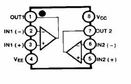
DUAL OPERATIONAL AMPLIFIER
FEATURES
• No frequency compensation required.
• No latch up.
• Large common mode and differential voltage range.
• Parameter tracking over temperature range.
• Gain and phase match between amplifiers.
• Internally frequency compensated.
• Low noise input transistors.
BLOCK DIAGRAM
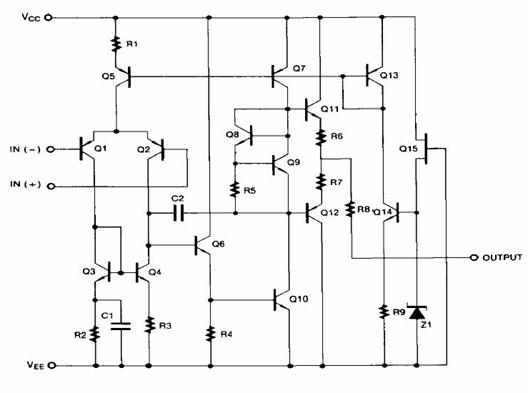
PIN DESCRIPTION
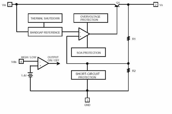
LOW DROPOUT VOLTAGE REGULATOR
DESCRIPTION
The KA78R05 is a low-dropout voltage regulator suitable for various electronic equipments. It provides constant voltage power source with TO-220 4 lead full mold package.
Dropout voltage of KA78R05 is below 0.5V in full rated current(1A). This regulator has various function such as peak current protection, thermal shut down, overvoltage protection and output disable function.
FEATURES
• 1A / 5V Output low dropout voltage regulator
• TO220 Full-Mold package (4PIN)
• Overcurrent protection, Thermal shutdown
• Overvoltage protection, Short-Circuit protection
• With output disable function
BLOCK DIAGRAM
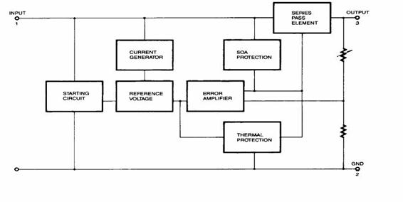
3 TERMINAL 1A POSIIVE VOLTAGE REGULATOR
DESCRIPTION
The KA78XX/KA78XXA series of three-terminal positive regulator are available in the TO-220/D-PAK package and with several fixed output voltages, making them useful in a wide range of applications. Each type employs internal current limiting, thermal shut down and safe operating area protection, making it essentially indestructible. If adequate heat sinking is provided, they can deliver over 1A output current. Although designed primarily as fixed voltage regulators, these devices can be used with external components to obtain adjustable voltages and currents.
FEATURES
• Output Current up to 1A
• Output Voltages of 5, 6, 8, 9, 10, 12, 15, 18, 24V
• Thermal Overload Protection
• Short Circuit Protection
• Output Transistor Safe Operating Area Protection
BLOCK DIAGRAM
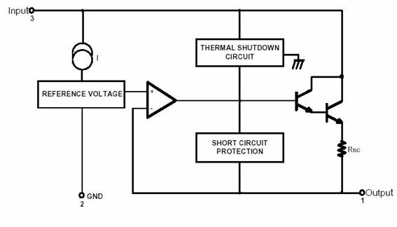
3 TERMINAL 0.1A NEGATIVE VOLTAGE REGULATOR
DESCRIPTION
The KA78LXXA/KA78L05AA series of fixed voltage monolithic integrated circuit voltage regulators are suitable for application that required supply current up to 100mA.
FEATURES
• Maximum Output Current of 100mA
• Output Voltage of 5V, 6V, 8V, 9V,10V, 12V, 15V, 18V and 24V
• Thermal Overload Protection
• Short Circuit Current Limiting
• Output Voltage Offered in ¡¾5% Tolerance
BLOCK DIAGRAM
VOLTAGE DETECTOR
DESCRIPTION
The KA75250/KA75270/KA75290/KA75310/KA75330/KA75360/KA75390/KA75420/KA75450 prevents the error of system from supply voltage below normal voltage level at the time the power on and instantaneous power off in systems.
FEATURES
• Detecting Against Error Operations At The Power On/off.
• Resetting Function For The Low Voltage Microprocessor.
• Checking Low
BLOCK DIAGRAM
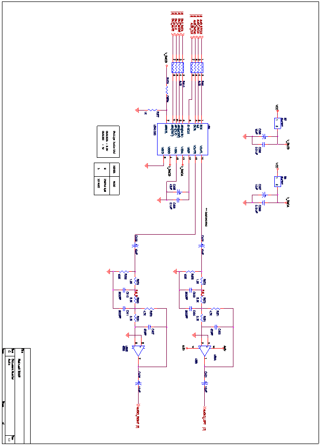
DIGITAL CHANNEL MODULE
FEATURES
950 ~ 2150 MHz tuning range
2 ~ 45M symbol rate supported, thus suitable for SCPC and MCPC application
Internal AGC monitor out
I2C-bus control for tuner PLL and for LINK IC
Loop through output
Both parallel and serial output transport stream interface
22KHz tone output for LNB and DiSEqC
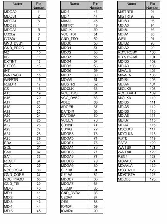
PIN DESCRIPTION
|
PIN NO. |
MARK |
DESCRIPTION |
CURRENT (typ) |
RIPPLE(max) |
|
|
LNBA |
Power input for LNB A |
|
|
|
|
LNBB |
LNB from |
|
|
|
|
5V_RF |
5V for RF-AMP and loop through |
20mA |
20mVp-p |
|
|
AGC |
AGC monitor |
|
|
|
|
5V_ZIF |
5V for 2nd AMP and ZIF IC |
80mA |
20mVp-p |
|
|
VT |
30V tuning voltage |
|
|
|
|
5V_PLL |
5V for ZIF IC, PLL IC and OSC |
130mA |
20mVp-p |
|
|
I |
I signal monitor |
|
|
|
|
Q |
Q signal monitor |
|
|
|
|
PORT2 |
I/O |
|
|
|
A |
5VAGC |
Power of AGC AMP |
10mA |
20mVp-p |
|
B |
GND |
Ground |
|
|
|
C |
3.3V |
Power of LINK IC |
200mA |
20mVp-p |
|
D |
F22 |
22KHz tone output |
|
|
|
E |
AUX_CLK |
Bypassed sampling clock(60MHz) |
|
|
|
F |
RESET |
Reset (active LOW) |
|
|
|
G |
ERROUT |
Frame error output (active HIGH) |
|
|
|
H |
FRAME_SYNC |
Frame sync. (active HIGH) |
|
|
|
I |
DATA_VALID |
Data valid (active HIGH) |
|
|
|
J |
DATA_CLK |
Data clock (falling edge triggering) |
|
|
|
K~R |
DATA0~7 |
Byte data |
|
|
|
S |
SDA |
I2C serial data |
|
|
|
T |
SCL |
I2C serial clock |
|
|
BLOCK DIAGRAM
RF MODULATOR
FEATURES
This specification outlines the pertinent electrical requirements of the RF output modulator which converts the TV video and TV audio signal into the RF signal for PAL G.I.K color television.
GENERAL DESCRIPTION
|
Item |
Specification |
|
Output channel |
21~69CH. |
|
Power supply |
MOD. : 5 0.25V DC Ripple 5mVp-p MAX Vt : 30V 2V DC Ripple 5mVp-p MAX |
|
Consumption current |
MOD. : MAX. 90mA Vt : MAX 5mA Booster : MAX. 40Ma |
|
Operationg temperature range |
Temperature 5 to 65 C, Humidity 80% |
|
Storage temperature range |
Temperature –10 to 70 C, Humidity 80% |
|
Wave flow soldering |
C for 10 seconds |
|
The limits of performance guarantee |
This specification is applied to ch.40 except channels pointed out especially. Besides it is guarantee that the other channels fit for practical USE. |
|
Others |
If there are any doubts regarding the specification or the products, It will be settled by consultation between samsung and the customer. |
|
ESD protection |
4 kV (at RF output connectors) |
Supports Mixed-Mode Signal Operation(5-V Input and Output Voltages With 3.3-V VCC)
Supports
Unregulated
Typical VOLP (Output Ground Bounce) <0.8 V at VCC = 3.3 V, TA = 25 C
Ioff and Power-Up 3-State Support Hot Insertion
Latch-Up Performance Exceeds 100 mA Per JESD 78, Class II
ESD Protection Exceeds JESD 22
- 2000-V Human-Body Model (A114-A)
- 200-V Machine Model (A115-A)
- 1000-V Charged-Device Model (C101)
description/ordering information
This octal bus transceiver is designed specifically for low-voltage (3.3-V) VCC operation, but with the capability
to provide a TTL interface to a 5-V system environment.
The SN74LVT245B is designed for asynchronous communication between data buses. The device transmits
data from the A bus to the B bus or from the B bus to the A bus, depending on the logic level at the
direction-control (DIR) input. The output-enable (OE) input can be used to disable the device so the buses are
effectively isolated.
Part Number : ST340015ACE
Capacity: : 40 GB
Speed: : 5400 rpm
Seek time: : 12.5 ms avg
Interface: : Ultra ATA/100
Description
Barracuda 5400.1 delivers a cost-efficient design with features you would expect from a more expensive drive. Whether integrating into an entry-level PC or consumer electronics application, Barracuda 5400.1 is the ideal solution for cost-sensitive systems
Features
SoftSonic FDB motor
Enhanced G-Force Protection
SeaTools Suite diagnostic software
5400 RPM performance level
Benefits
Enables whisper-quiet acoustics and increased reliability.
New mechanical enhancements further protect the drive from nonoperating shock.
Software available for free download at seatools.seagate.com that reduces unnecessary returns up to 40%. Diagnoses Seagate and other manufacturers' drives, and helps to identify or eliminate the drive as a source of system issues.
Delivers excellent performance for most PC and CE applications at a great value.
|
Pin |
I/O |
Signal Name |
Pin |
I/O |
Signal Name |
|
|
I |
-RESET |
|
N/A |
Ground |
|
|
I/O |
D7 |
|
O |
D8 |
|
|
I/O |
D6 |
|
O |
D9 |
|
|
I/O |
D5 |
|
O |
D10 |
|
|
I/O |
D4 |
|
O |
D11 |
|
|
I/O |
D3 |
|
O |
D12 |
|
|
I/O |
D2 |
|
O |
D13 |
|
|
I/O |
D1 |
|
O |
D14 |
|
|
I/O |
D0 |
|
O |
D15 |
|
|
NA |
Ground |
|
NA |
(key) |
|
|
NA |
Reserved |
|
NA |
Ground |
|
|
I |
-IOW |
|
NA |
Ground |
|
|
I |
-IOR |
|
NA |
Ground |
|
|
O |
IORDY |
|
NA |
Reserved |
|
|
NA |
Reserved |
|
NA |
Ground |
|
|
O |
IRQ |
|
O |
-IOCS16 |
|
|
I |
A1 |
|
I/O |
-PDIAG |
|
|
I |
A0 |
|
I |
Dev.-addr. A2 |
|
|
I |
-HFCS0 |
|
I |
-HFCS1 |
|
|
NA |
-DASP |
|
NA |
Ground |
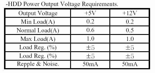
TABLE1
NOTICE
1) We recommend to repair on board level, because SMPS can damage to body & equipment.
2) As the Primary(charge) part that can damage to body is high voltage, put on insulator globe.
3) If each component is short, a serious problem will occur. So when treating SMPS, have to take care.
4) The GND between the Primary(charge) part and the Secondary(discharge) part is separated.
So to protect damage in using equipment, be careful to connect each GND point.
5) The Primary parts is operated at high voltage.
When measuring the Primary part, use a special probe and do not touch and short.
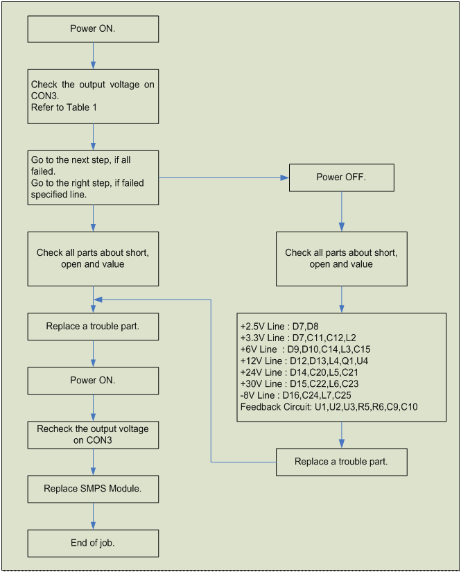
STEP 1. Check power supply on board level
-. If not work STB, replace a new SMPS.
-. If STB is work, classify it as a trouble SMPS
STEP 2. Check the Secondary part.(Right side of transformer)
![]()
![]()
![]()
![]()
![]()
![]()
![]()
|
