Sound systems
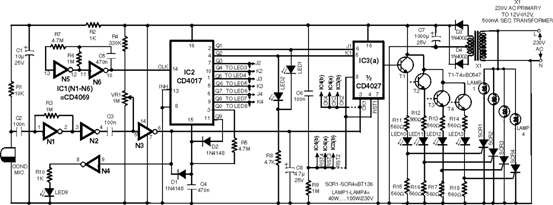
Clap Remote
An infra-red or wireless remote control has the disadvantage that the small, handy, remote transmitter is often
misplaced. The sound operated switch has the advantage that the transmitter is always with you. This project
offers a way to control up to four latching switches with two claps of your hand. These switches may be used to
control lights or fans - or anything else that does not produce too loud a sound. To prevent an occasional loud
sound from causing malfunction, the circuit is normally quiescent. The first clap takes it out of standby state and
starts a scan of eight panel-mounted LEDs. Each of the four switches are accompanied with two LEDs - one
for indicating the 'on' and the other for indicating the 'off' state. A second clap, while the appropriate LED is lit,
activates that function. For example, if you clap while LED10 used in conjunction with Lamp 1 is lit then the
lamp turns on. (If it is already on, nothing happens and it remains on.) A condenser microphone, as used in
tape recorders, is used here to pick up the sound of the claps. The signal is then amplified and shaped into a
pulse by three inverters (N1 through N3) contained in CMOS hex inverter IC CD4069. A clock generator built
from two of the inverter gates (N5 and N6) supplies clock pulses to a decade counter CD4017 (IC2). Eight
outputs of this IC drive LEDs (1 through 8). These outputs also go to the J and K inputs of four flip-flops in two
type CD4027 ICs (IC3 and IC4). The clock inputs of these flip-flops are connected to the pulse shaped sound
signal (available at the output of gate N3). Additional circuitry around the CD4017 counter ensures that it is in
the reset state, after reaching count 9, and that the reset is removed when a sound signal is received. Outputs
of the four flip-flops are buffered by transistors and fed via LEDs to the gates of four triacs. These triacs switch
the mains supply to four loads, usually lamps. If small lamps are to be controlled, these may be directly driven
by the transistors. If this circuit is to be active, i.e. scanning all the time, some components around CD4017 IC
could be omitted and some connections changed. But then it would no longer be immune to an occasional,
spurious loud sound. The condenser microphone usually available in the market has two terminals. It has to be
supplied with power for it to function. Any interference on this supply line will be passed on to the output. So the
supply for the microphone is smoothed by resistor-capacitor combination of R2, C1 and fed to it via resistor
R1. CD4069, a hex unbuffered inverter, contains six similar inverters. When the output and input of such an
inverter is bridged by a resistor, it functions as an inverting amplifier. Capacitor C2 couples the signal
developed by the microphone to N1 inverter in this IC, which is configured as an amplifier. The output of gate
N1 is directly connected to the input of next gate N2. Capacitor C3 couples the output of this inverter to N3
inverter, which is connected as an adjustable level comparator. Inverter N4 is connected as an LED (9) driver
to help in setting the sensitivity. Preset VR1 supplies a variable bias to U3. If the wiper of VR1 is set towards
the negative supply end, the circuit becomes relatively insensitive (i.e. requires a thunderous clap to operate).
As the wiper is turned towards resistor R4, the circuit becomes progressively more sensitive. The sound signal
supplied by gate N2 is added to the voltage set by preset VR1 and applied to the input of gate N3. When this
voltage crosses half supply voltage, the output of gate N3 goes low. This output is normally high since the input
is held low by adjustment of preset VR1. This output is used for two things: First, it releases the reset state of
IC2 via diode D1. Second, it feeds the clock inputs to the four flip-flops contained in IC3 and IC4. In the
quiescent state, IC2 is reset and its 'Q0' output is high. Capacitor C4 is charged positively and it holds this
charge due to the connection from R5 to this output (Q0). IC2 is a decade counter with fully decoded outputs. It
has ten outputs labelled Q0 to Q9 which go successively high, one at a time, when the clock in put is fed with
pulses. IC3 and IC4 are dual JK flip-flops. In this circuit they store (latch) the state of the four switches and
control the output through transistors and triacs. At the first clap, the output of gate N3 goes low. Diode D1 is
forward biased and it conducts, discharging capacitor C4. The reset input of IC2 goes low, releasing its reset
state. All the J and K inputs of the four flip-flops are low and so these do not change state, even though their
clock inputs receive pulses. When the reset input of IC2 is low, each clock pulse causes IC2 to advance by one
count and its outputs go high successively, lighting up the corresponding LEDs and pulling high the J and K
inputs of the four flip-flops, one after the other. Resistor R8 limits the current through LEDs 1 through 8 to about
2 mA. Larger current might cause malfunction due to the outputs of IC2 being pulled down below the logic 1
state input voltage. If a second clap is detected while the J input of a particular flip-flop is high, its Q output will
go high, regardless of what state it was in previously. Similarly, if its K input was high, the output will go low. (If
both J and K are high, the output will change state at each clock pulse.) Thus although all flip-flops receive the
clap signal at their clock inputs, only the one selected by the active output of IC2 will change state. Resistor R9
and capacitor C6 ensure that the flip-flops start in the off state when power to the circuit is switched on, by
providing a positive power-on-reset pulse to the reset input pins when power is applied. The preset input pins
are not used and are therefore connected directly to ground. When, after eight clock pulses, output Q8 of IC2
becomes high, diode D2 conducts, charging capacitor C4, thereby resetting IC2 and making its Q0 output
high. And there it stays, awaiting the next clap. The four Q outputs of IC3 and IC4 are buffered by npn
transistors, fed through current limiting resistors and LEDs (to indicate the on/off state of the loads) to the
gates of four triacs. Four lamps operating on the mains may thus be controlled. For demonstrations, it might be
better to drive small lamps (drawing less than 100 mA at 12V) directly from the emitters of the transistors. In
this case the triacs, LEDs and their associated current limiting resistors may be omitted. It has to be noted that
one side of the mains has to be connected to the negative supply line of this circuit when mains loads are to be
controlled. This necessitates safe construction of the circuit such that no part of it is liable to be touched. The
advantage is that it may be mounted out of reach of curious hands since it does not need to be handled during
normal operation. It is advisable to start with the low voltage version and then upgrade to mains operation,
once you are sure everything else is working satisfactorily. CMOS ICs are used in this circuit for implementing
the amplifying and logic functions. Use of a dedicated supply is recommended because the integrated circuits
will be damaged if the supply voltage is too high, or is of wrong polarity. An external power supply may get
connected up the wrong way around, or be inadvertently set to too high a voltage. Therefore it is a good idea to
start by constructing the power supply section and then add the other components of the circuit. If the clock is
working, you may turn your attention to the amplifier. LED9 should be off, and should flash when the terminals
of capacitor C2 are touched with a wet finger (the classic wet finger test). Preset VR1 may need to be
adjusted until LED9 just turns off. The output of gate N2 will be at about half the supply voltage. The output of
gate N3 would normally be high. The voltage at the input of gate N3 should vary when preset VR1 is varied.
High-efficiency LEDs should preferably be used in this circuit. The microphone has two terminals, one of which
is connected to its body. This terminal has to be connected to circuit ground, and the other to the junction of
resistor R2 and capacitor C2. These wires are preferably kept short (one or two centimetres) to avoid noise
pickup. With the microphone connected, a loud sound (a clap) should result in LED9 blinking. Adjust preset
VR1 so that LED9 stays off on the loudest of background noises but starts glowing when you clap. If the
clap-to-start feature is not required, it may be disabled by omitting components D1, D2, R5, C4 and
connecting a wire link in place of diode D2. Then IC2 will be alive and kicking all the time. .
Colour Sensor
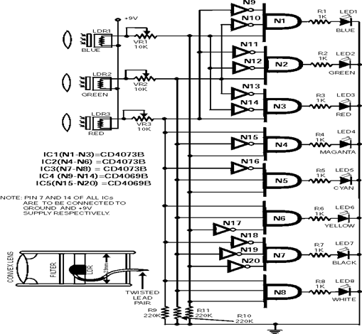
Colour sensor is an interesting project for hobbyists. The cir- cuit can sense eight colours, i.e. blue, green and
red (primary colours); magenta, yellow and cyan (secondary colours); and black and white. The circuit is based
on the fundamentals of optics and digital electronics. The object whose colour is required to be detected
should be placed in front of the system. The light rays reflected from the object will fall on the three convex
lenses which are fixed in front of the three LDRs. The convex lenses are used to converge light rays. This helps
to increase the sensitivity of LDRs. Blue, green and red glass plates (filters) are fixed in front of LDR1, LDR2
and LDR3 respectively. When reflected light rays from the object fall on the gadget, the coloured filter glass
plates determine which of the LDRs would get triggered. The circuit makes use of only 'AND' gates and 'NOT'
gates.
When a primary coloured light ray falls on the system, the glass plate corresponding to that primary colour will
allow that specific light to pass through. But the other two glass plates will not allow any light to pass through.
Thus only one LDR will get triggered and the gate output corresponding to that LDR will become logic 1 to
indicate which colour it is. Similarly, when a secondary coloured light ray falls on the system, the two primary
glass plates corres- ponding to the mixed colour will allow that light to pass through while the remaining one will
not allow any light ray to pass through it. As a result two of the LDRs get triggered and the gate output
corresponding to these will become logic 1 and indicate which colour it is.
When all the LDRs get triggered or remain untriggered, you will observe white and black light indications
respectively. Following points may be carefully noted :
1. Potmeters VR1, VR2 and VR3 may be used to adjust the sensitivity of the LDRs.
2. Common ends of the LDRs should be connected to positive supply.
3. Use good quality light filters.
The LDR is mounded in a tube, behind a lens, and aimed at the object. The coloured glass filter should be
fixed in front of the LDR as shown in the figure. Make three of that kind and fix them in a suitable case.
Adjustments are critical and the gadget performance would depend upon its proper fabrication and use of
correct filters as well as light conditions.
Digital Switching System
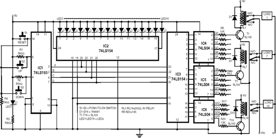
This circuit can control any one out of 16 devices with the help of two push-to-on switches. An up/down counter
acts as a master-controller for the system. A visual indication in the form of LEDs is also available. IC1
(74LS193) is a presettable up/down counter. IC2 and IC3 (74LS154) (1 of 16 decoder/demultiplexer) perform
different functions, i.e. IC2 is used to indicate the channel number while IC3 switches on the selected channel.
Before using the circuit, press switch S1 to reset the circuit. Now the circuit is ready to receive the input clock.
By pressing switch S2 once, the counter counts up by one count. Thus, each pressing of switch S2 enables the
counter to count up by one count. Likewise, by pressing switch S3 the counter counts downwards. The counter
provides BCD output. This BCD output is used as address input for IC2 and IC3 to switch one (desired
channel) out of sixteen channels by turning on the appropriate triac and the corresponding LED to indicate the
selected channel. The outputs of IC3 are passed through inverter gates (IC4 through IC6) because IC3
provides negative going pulses while for driving the triacs we need positive-going pulses. The high output of
inverter gates turn on the npn transistors to drive the triacs. Diodes connected in series with triac gates serve
to provide unidirectional
current for the gate-drive.
Versatile Variable
Duration Digital Timer
Here is a versatile
on-off (or off-on)
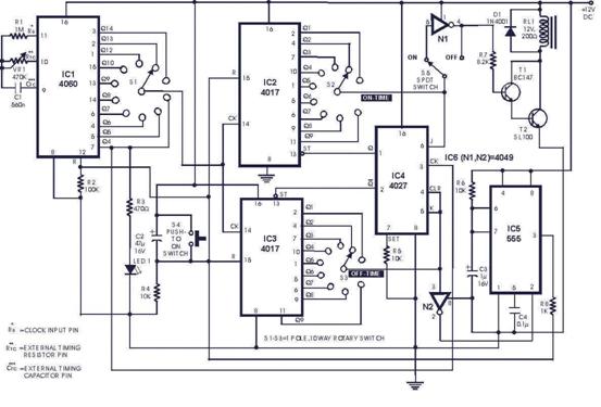
timer circuit. Its time delay can be set from seconds to hours. The time for which the circuit will remain on (or off) can be selected with the help of switch S2. This will be followed by off (or on) state lasting for a period which can be selected with the help of switch S3. Thus the load or device will be initially on (or off) for certain selected duration after which the intial state will toggle to off (or on) state for another selected duration. Thereafter the cycle will repeat. Switch S1 in conjunction with potentiometer VR1 can be used for varying the overall cycle duration (on and off periods or the other way around) without disturbing the on to off (or off to on) ratio determined by switches S2 and S3.
IC1 (4060) functions as an oscillator and 14-stage binary counter. The oscillator timing is so adjusted with the help of VR1 that a pulse repitition rate of one hour is obtained at its final output pin 3 (Q14 output). The outputs Q1 through Q14 are square waves, i.e. their on and off periods are equal. The pulse repetition rates of Q13, Q12, Q11.... will accordingly be 1/2,
1/4, 1/8..... (hour) respectively. One of the outputs of IC1 selected with the help of switch S1 serves as clock for IC2 and IC3 which are both Johnson ring counters (4017). IC2 is used for the initial on or off time setting. After it counts the
number of pulses it is set for, it produces a low-to-high going output. If you want a device or load operated via relay RL1 to be initially off then flip switch S5 to position marked 'off'. If the relay is to be initially in on position, flip switch S5 to on position as shown in the circuit. Transistors T1 and T2 form a darlington pair for driving the relay.
On power-on, a reset pulse developed across resistor R4 resets IC1, IC2, and IC3. Also Q output at pin 1 of IC4 flip-flop is low which enables IC2, while Q output at pin 2 being high keeps IC3 inhibited.
Assuming switch S5 to be in 'on' postion, the output of inverter N1 is initially high and the relay gets energised. At the end of the selected period (through switch S2), output of IC2 goes high and that of inverter N1 goes low. As a result relay gets de-energised and simultaneously J-K flip-flop toggles enabling IC3 and inhibiting IC2. Thus IC3 starts advancing and when the period selected via switch S3 is completed, the output at pole of switch S3 goes high.
This low-to-high input is converted into high-to-low going voltage at the output of inverter N2. This triggers IC5 (555) which is configured to operate as monostable multivibrator. The high output pulse from pin 3 of IC5 is used as reset pulse for IC1 through IC3. As a result the circuit returns to its initial conditions and the entire operation repeats.
Manual resetting of the circuit is possible by momentary depression of switch S4.
Important points concerning the operation of the circuit are:
1. On/off sequence can be changed to off/on sequence using switch S5.
2 Maximum 'on' and 'off' time selectable is 10 hours, unless values of timing components ie preset VR1 and capacitor C1 are altered.
Switch S1 in fact determines the timer resolution while switches S2 and S3 determine "how many times?" If S1 is connected to Q14 (pin 1) of IC1 and if S2 is in position 5, and S3 is in position 7, the initial on (or off) period is 5 hours followed by off (or on) period of 7 hours. When S1 is connected to Q8, the resolution is approx. one minute.
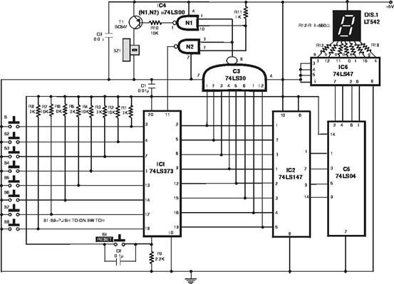
Electronic Jam
This jam circuit can be used in quiz contests wherein any par- ticipant who presses his button (switch) before
the other contestants, gets the first chance to answer a question. The circuit given here permits up to eight
contestants with each one allotted a distinct number (1 to 8). The display will show the number of the
contestant pressing his button before the others. Simultaneously, a buzzer will also sound. Both, the display as
well as the buzzer have to be reset manually using a common reset switch. Initially, when reset switch S9 is
momentarily pressed and released, all outputs of 74LS373 (IC1) transparent latch go 'high' since all the input
data lines are returned to Vcc via resistors R1 through R8. All eight outputs of IC1 are connected to inputs of
priority encoder 74LS147 (IC2) as well as 8-input NAND gate 74LS30 (IC3). The output of IC3 thus becomes
logic 0 which, after inversion by NAND gate N2, is applied to latch-enable pin 11 of IC1. With all input pins of
IC2 being logic 1, its BCD output is 0000, which is applied to 7-segment decoder/driver 74LS47 (IC6) after
inversion by hex inverter gates inside 74LS04 (IC5). Thus, on reset the display shows 0. When any one of the
push-to-on switches-S1 through S8-is pressed, the corresponding output line of IC1 is latched at logic 0
level and the display indicates the number associated with the specific switch. At the same time, output pin 8
of IC3 becomes high, which causes outputs of both gates N1 and N2 to go to logic 0 state. Logic 0 output of
gate N2 inhibits IC1, and thus pressing of any other switch S1 through S8 has no effect. Thus, the contestant
who presses his switch first, jams the display to show only his number. In the unlikely event of simultaneous
pressing (within few nano-seconds difference) of more than one switch, the higher priority number (switch no.)
will be displayed. Simultaneously, the logic 0 output of gate N1 drives the buzzer via pnp transistor BC158
(T1). The buzzer as well the display can be reset (to show 0) by momentary pressing of reset switch S9 so that
next round may start. Lab Note: The original circuit sent by the author has been modified as it did not jam the
display, and a higher number switch (higher priority), even when pressed later, was able to change the
displayed number.
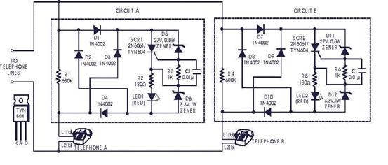
Extension Phone Switcher
Having multiple extension tele-
phones at home is very conve-
nient. You can make or receive phone calls practically anywhere in the house. This circuit disables other telephones connected to the phone line whenever a telephone (either the master or any extension phone) is in use. The circuit is inexpensive and is guaranteed to keep the phone conversation private.
The circuit does not need an external power supply. It gets its power from the telephone line. The no-load voltage at the telephone line, when the telephone handset is 'on-hook,' is around 48 volts. However, when the handset is off-hook, terminal voltage drops to between 5 volts and 15 volts. This is due to the impedance of telephone line and the telephone set. The voltage of the telephone line is the key factor that controls the operation of this circuit.
diodes D1, D2, D3 and D4 are connected as bridge rectifier to make the circuit non-polarised. Lifting the handset causes the terminal voltage to drop from 48V to about 10V. The drop in voltage does not, however, occur rapidly. therefore while the terminal voltage is still high (above the threshold voltage level), both zener diodes D5 and D6 are turned on. Current flows through resistor R3, triggering SCR1 and providing a link to the telephone set connected to lines L1(a) and L2(a).
When the terminal voltage drops below the threshold voltage of the zener diode, diode D5 reverts to its non-conducting state, cutting off the gate drive to SCR1. However, once the SCR is on, it will remain in that state as long as the current flowing through it does not fall to near zero level. Thus the link continues. Zener D6 maintains the voltage across resistor R2 and LED1/LED2 indicates as to which telephone is in use.
The low off-hook voltage of the line will disable the other extension phones. The line voltage will not turn on zener diodes D11 and D12, even if the handsets of the other extension phones are lifted.
Use the following procedure to check up the system after wiring:
1. Lift the handset of each telephone to see whether the corresponding LED lights up. Return the handset back in its cradle; the LED should turn off. Use the same procedure to check the other phones.
2. Lift the handset of phone 'A;' its corresponding LED should light up. The other phones should be cut-off (no dial tone).
3. Lift the
handset of phone 'B', then return the handset of phone
'A' to its cradle. Now 'B' telephone's LED should light up and the dial tone
should be heard through the ear-piece.
Single-IC decoy switch
Adecoy switch is used to create
a virtual impression of occu-
pancy of a vacant house. Generally when we leave our premises, we are in a dilemma as to whether to leave the lights on or keep them off. In either case anyone (may be a burglar) watching the house from a distance for some time could easily guess that there is no one in the house as he would not see any activity. This is based on the hypothesis that when someone is present in the house, some gadgets are switched on or off, e.g. lights are turned on or off at irregular intervals.
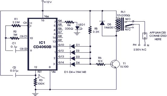
Here is a way to create an impression that there is someone present in the house. In the circuit described here any appliance connected across the points shown in the figure would get switched on after about an hour of switching on of the circuit. It would stays on for about 100 seconds, then go off for about the same duration, come on again for 100 seconds and again go off for about an hour, and this cycle continues untill the circuit is switched off. A light or a radio or a TV set connected to the abovementioned output terminals would follow this sequence and give an impression that someone is present in the house.
The circuit needs just a single IC, four diodes, a relay with a driver transistor and a couple of resistors and capacitors. All these can be easily accommodated in a small container such as a soap box. As seen from the circuit, resistors R1, R2 and capacitor C1 determine the oscillator and internal clocking frequency for the binary counter/oscillator IC CD4060B (IC1). The capacitor-resistor combination of C2-R3 provides the power-on-reset (POR) pulse needed to start the outputs from '0' state.
Long duration timing of IC1 is effectively selected by ANDing Q10, Q12, Q13 and Q14 outputs which give a very large value of time interval since the counting is in binary fashion. Note that there is no Q11 output for this IC. This fact is effectively used here to generate two 'on' signals, corresponding to Q11 'on' period for driving relay RL1.
Diodes D1-D4 connected in the fashion shown form a logic AND circuit, and when all the four outputs go high then transistor T1 is driven to saturation. When any one of the outputs is low, the base is pulled to '0' state via any one of the conducting diodes and the transistor is switched off.
'On' state of transistor T1 occurs twice in a full cycle as Q10 output goes high-and-low twice when other outputs (Q12, Q13 and Q14) are all high. Correspondingly, relay RL1 switches on twice. The contact ratings of the relay should be capable of handling the load to be connected.
In fact this circuit can be used with wide variations to generate various timing durations. By changing the values of resistors R1 and/or R2, or by substituting a potentiometer in one of these arms, additional timings are possible. Further, by changing capacitor C1's value some additional timings can be obtained.
Table I gives approximate time periods with capacitor C1 = 0.1µF and when capacitor C1's value is doubled (by connecting two 0.1µF capacitors in parallel). Depending on the application this circuit can be advantageously used by combining various outputs as desired. The timing given in the table are the actual measured values (by the author).
It is seen that at higher values of capacitors the timings are not very accurate. Also, capacitor tolerances give inaccurate readings. However, in this particular application, it is not required to have very precise timings. In fact if the timings change a little, it is better, because a sort of randomness is added to the on and off timings.
Also note that this is a high voltage series (B series) IC for which the supply voltage can go up to about 18V without damaging the IC. So there is no need for a regulator-a simple 12V rectified and filtered DC would be good enough to operate this circuit.
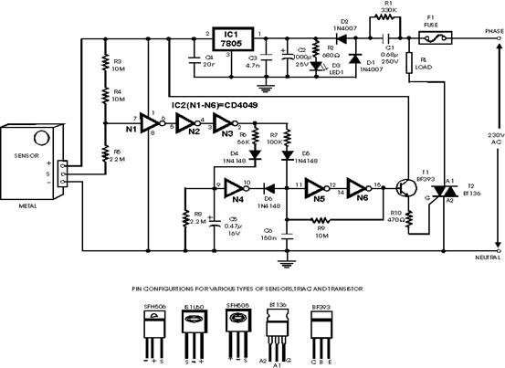
Here is a
circuit
which can switch on and switch off any
appliance with the help of a common type of infra-red remote control (transmitter). This circuit senses the IR pulse and then controls the appliance accordingly. The circuit functions such that a short pulse from the remote tran- smitter switches on the triac (and the load) while a longer pulse switches off the triac as also the load.
The circuit is built around hex inverter IC CD 4049. When the infra-red pulse is received by the sensor, its output (Note: Here VR1 denotes the in-circuit resistance of preset VR1.)
The output of multivibrator is fed to the base of current amplifier 2N3055 via resistor R2 (1kilo-ohm). The brakelight bulb is connected in series with the collector of 2N3055. The flashing rate of this bulb is adjusted by 100k preset (VR1). Transistor 2N3055 may get heated due to high current switching action; hence a small heatsink, similar to the type used in television power supply, is recommended.
The category of 2-wheelers which do not have a battery, can use the bridge rectifier circuit shown here. Several designs of round, square and rectangular reflectors are available which may be used in conjunction with any suitable 12V bulb with proper rating (around 20 watts).
However, if flashing of the brake- light affects intensity of headlight bulb, reduce the rating of brakelight bulb to 10 watts.

Intelligent switch
This
intelligent switch circuit en- ables automatic switching on of an emergency
light system during darkness in the event of mains failure. The mains
power failure condition is detected by the section consisting of mains
step-down transformer X1 followed by bridge rectifier comprising diodes D1
through D4 and smoothing capacitor C1. If the mains is
available then it causes energisation of relay RL1 which has two sets of
changeover contacts. The light/darkness condition is detected by the circuit
comprising photo-transistor FPT100/2N5777 followed by
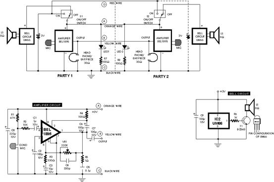
The circuit of a two-position in-
tercom is presented here. This
circuit is very simple yet it functions quite satisfactorily. The circuit does not involve any complicated switching. The switches S1/S2 must be fixed in such a way that when the handset is resting on the cradle, the switch is OFF and when it is taken off the cradle, the switch turns on.
Both the sets used are identical in construction. When one set (say, party 1) is switched on, the other set's (party 2's) bell ener- gises. When party 2 turns on his own set, his bell automatically stops and he can talk to party 1 via his microphone. One can substitute the BEL 1895 IC based amplifier and bell circuit with any other low power amplifier and bell circuit. The block diagram clarifies the connection of the two sets.
Only three wires are required to connect the two sets if se- parate ba- ttery is us- ed in each set. However, if the battery is common for the two sets, it requires four wires for interconnections.
The circuit
can be easily assembled on a general-purpose PCB. Intercom cases are also available
in the market which may be used for giving it a professional outlook.
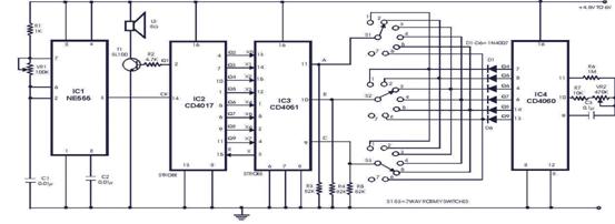
The circuit presented here is that
of a musical bell which may be
programmed for generation of a number of musical notes. The complete working of the circuit is explained below.
IC1 timer (NE555) is wired as an astable multivibrator operating in audio band. Frequency of the timer IC may be varied with the help of potmeter VR1. The output of IC1 at the selected frequency of operation is coupled to the clock input of IC2 (CD4017). IC2 divides the input frequency by an integer 'n'. The value of 'n' depends on its output pin number which is connected to its own reset pin 15. In this circuit the maximum value of 'n' that may be selected is 8. This selection is carried out with the help of CD4051 (IC3) which is a CMOS 8-input analogue multiplexer whose function here is to make an electrical connection between specified output of IC2 and pin 15 of IC2 . The output of IC2, which is connected to its pin 15, depends on the binary number present at the address input pins 9 through 11 of IC3 CD4051. Thus by changing the binary number applied to the address control input of IC3, the value of 'n' as also the frequency division ratio can be changed.
The final output Q1 after frequency division available at pin 2 of IC2 is amplified by transistor T1(SL100). Different frequency division ratios produce different tones from the speaker. The different tones are connected serially in a particular sequence to produce various musical notes. This is achieved through IC4 (CD4060) which is a 14-bit binary counter. Delay time of tone is adjusted with the help of potmeter VR2. Changing the arrangement of tones in the sequence (and also the delay introduced in each tone) will result into different musical notes. Switches S1, S2 and S3 serve this purpose.
Try different positions of switches S1, S2 and S3 and delay control potmeter VR2 to abtain different notes into the speaker. Use potmeter VR1 to change the tone.
Accurate Electronic Stop-Watch
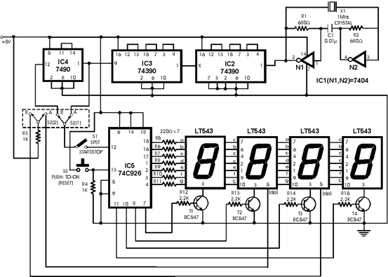
Here is a simple circuit which can be used as an accurate stop-watch to count up to 100 seconds with a
resolution of 0.01 second or up to 1000 seconds with a resolution of 0.1 second. This stop-watch can be used
for sports and similar other activities. A 1MHz crystal generates stable frequency which is divided by two
stages of 74390 ICs (dual decade counter) and another stage employing 7490 (decade counter) IC to obtain a
final frequency of 100 Hz or 10 Hz. Due to the use of crystal, the final frequency is very accurate.
The output of IC4 (7490) is counted and displayed using IC 74C926 (4-digit counter with multiplexed
7-segment LED driver). Due to multiplexed display the power consumption is very low. Switch S2 (2-pole,
2-way) is used to select appropriate input frequency and corresponding decimal point position to display up to
either 99.99 seconds or 999.9 seconds maximum count.
For proper operation, first press switch S3 (reset) and then operate switch S2, according to the
resolution/range desired (0.1 sec. or 0.01 sec.) 100 seconds or 1000 seconds). Now to start counting, press
switch S3. To stop counting, press switch S3 again. The counting will stop and display will show the correct
time elapsed since the start of counting.
Sensitive Temperature Switch
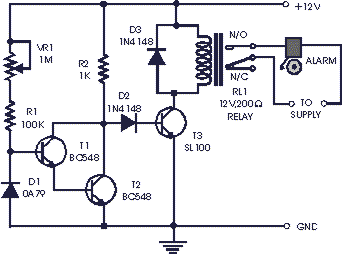
This temperature switch has a
high sensitivity and is quite re-
liable.
Here, in place of a single transistor, a
At normal room temperature germinum diode D1 (OA79 or equivalent) has a back
resistance value of about 10 kilo-ohms. As a result
But when temperature increases, the back resistance of diode D1 decreases sharply,
which results in cutting off of
This simple circuit can be used as an overheat indicator, fire alarm, or it can be used in a constant temperature circuit for switching on a fan etc. The circuit can be easily assembled on a piece of veroboard. Diode sensor D1 must be of germanium type and not silicon
Time Switch
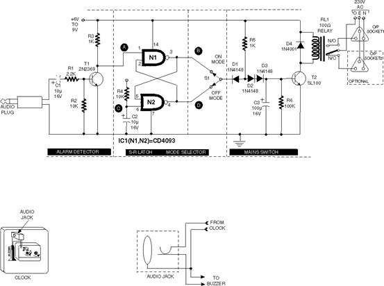
This circuit is especially designed for those who often need to wake up early in the morning. Ordinary alarms in
electronic watches are not loud enough and very often they fail to wake up. The switch circuit described here
will come handy; it can be used to switch on a TV, radio or tape recorder etc, which will not allow even the
laziest amongst us to ignore their sound for too long. Besides, this time switch can also be used to switch
on/off any other electric or electronic gadget at any time. What you need is a simple analogue electronic clock
with alarm facility and a small circuit to implement the time switch. This time switch has two modes. One is
'time-on' mode and the other is 'time-off' mode. In time-on mode, you set up the alarm in your clock as per
normal procedure and at the set time this switch turns on the gadget connected at the output socket-1. In
time-off mode, it turns your gadget off at the set time. The optional output socket-2 is wired in such a way that
when you use this socket, the mode changes without having to flip the mode switch (i.e. mode switch can be
omitted). Please refer to the back panel diagram of a typical analogue clock and the audio jack, to see how
the existing buzzer of the clock is required to be wired to the audio output from the clock. This will ensure that
when plug is inserted in the audio jack, the clock's buzzer will remain off and not consume any power
unnecessarily. The audio alarm output from the clock is coupled to the AF detector built around low-power
switching transistor T1. During alarm, the collector of transistor T1 will fluctuate around ground level and Vcc.
During absence of audio alarm input, the collector of transistor T1 is held at Vcc potential. The next stage
consists of an S-R latch built around NAND gates N1 and N2. Capacitor C2 and resistor R4 are used for
power-on-reset. On switching the power supply, gate N2 output will acquire logic 1 and that of gate N1 logic 0.
This is the initial state, irrespective of the position of mode switch. At the time of alarm, when point A
connected to collector of transistor T1 passes through logic 0 state, the output logic state of both the gates will
toggle. Assuming that mode switch is flipped to 'Mode Off' position at power-on-reset (when point D is at logic
1), initially diode D1 would be in blocking state and transistor T2 would be forward biased via resistor R5 and
diodes D2 and D3. As a result, the relay is in energised state, which makes output power available at output
socket-1 and cuts it off from socket-2. At alarm time, the audio signal toggles logic output states of both gates
N1 and N2. As a result, point D goes to logic 0 state. Diode D1 conducts, taking the voltage at junction of
diodes D1 and D2 to near about 1 volt. Diode D3 ensures that its series combination with diode D2 puts them
in blocking mode. Capacitor C3 meanwhile discharges via resistor R6 and the voltage at base of transistor T2
approaches towards ground level, cutting off transistor T2 and de-energising relay RL1. Now the power at
output socket-1 would be cut off while it becomes available in socket-2. If the above operation is repeated with
switch S1 in 'Mode On,' the power would initially not be available in socket-1 (but available in socket-2). But
after the alarm, the power would become available in socket-1 and not in socket-2. .
Tiny Dew Sensor
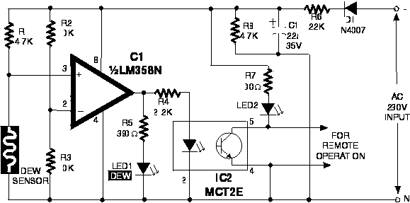
Dew (condensed moisture) ad- versely affects the normal per- formance of sensitive electronic devices. A
low-cost circuit described here can be used to switch off any gadget automatically in case of excessive
humidity. At the heart of the circuit is an inexpensive (resistor type) dew sensor element. Although dew sensor
elements are widely used in video cassette players and recorders, these may not be easily available in local
market. However, the same can be procured from authorised service centres of reputed companies. The
author used the dew sensor for FUNAI VCP model No. V.I.P. 3000A (Part No: 6808-08-04, reference no. 336)
in his prototype. In practice, it is observed that all dew sensors available for video application possess the
same electrical characteristics irrespective of their physical shape/size, and hence are interchangeable and
can be used in this project. The circuit is basically a switching type circuit made with the help of a popular dual
op-amp IC LM358N which is configured here as a comparator. (Note that only one half of the IC is used here.)
Under normal conditions, resistance of the dew sensor is low (1 kilo-ohm or so) and thus the voltage at its
non-inverting terminal (pin 3) is low compared to that at its inverting input (pin 2) terminal. The corresponding
output of the comparator (at pin 1) is accordingly low and thus nothing happens in the circuit. When humidity
exceeds 80 per cent, the sensor resistance increases rapidly. As a result, the non-inverting pin becomes
more positive than the inverting pin. This pushes up the output of IC1 to a high level. As a consequence, the
LED inside the opto-coupler is energised. At the same time LED1 provides a visual indication. The
opto-coupler can be suitably interfaced to any electronic device for switching purpose. Circuit comprising
diode D2, resistors R5 and R6 and capacitor C1 forms a low-voltage, low-current power supply unit. This
simple arrangement obviates the requirement for a bulky and expensive step-down transformer.
UltraSonic Switch
Circuit of a new type of remote
control switch is described
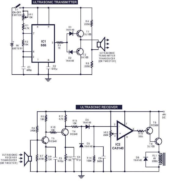
here. This circuit functions with inaudible (ultrasonic) sound. Sound of frequency up to 20 kHz is audible to human beings. The sound of frequency above 20 kHz is called ultrasonic sound. The circuit described generates (transmits) ultrasonic sound of frequency between 40 and 50 kHz.
As with any other remote control system this cirucit too comprises a mini transmitter and a receiver circuit. Transmitter generates ultrasonic sound and the receiver senses ultrasonic sound from the transmitter and switches on a relay.
The ultrasonic transmitter uses a 555 based astable multivibrator. It oscillates at a frequency of 40-50 kHz. An ultrasonic transmitter transducer is used here to transmit ultrasonic sound very effectively. The transmitter is powered from a 9-volt PP3 single cell.
The ultrasonic receiver circuit uses an ultrasonic receiver transducer to sense ultrasonic signals. It also uses a two-stage amplifier, a rectifier stage, and an operational amplifier in inverting mode. Output of op-amp is connected to a relay through a complimentary relay driver stage. A 9-volt battery eliminator can be used for receiver circuit, if required.
When switch S1 of transmitter is pressed, it generates ultrasonic sound. The sound is received by ultrasonic receiver transducer. It converts it to electrical variations of the same frequency.
These signals are amplified by transistors T3 and T4. The amplified signals are then rectified and filtered. The filtered DC voltage is given to inverting pin of op-amp IC2. The non-
inverting pin of IC2 is connected to a variable DC voltage via preset VR2 which determines the threshold value of ultrasonic signal received by receiver for operation of relay RL1.
The inverted output of IC2 is used to bias transistor T5. When transistor T5 conducts, it supplies base bias to transistor T6. When transistor T6 conducts, it actuates the relay. The relay can be used to control any electrical or electronic equipment.
Important hints:
1. Frequency of ultrasonic sound generated can be varied from 40 to 50 kHz range by adjusting VR1. Adjust it for maximum performance.
2. Ultrasonic sounds are highly directional. So when you are operating the switch the ultrasonic transmitter transducer of transmitter should be placed towards ultrasonic receiver transducer of receiver circuit for proper functioning.
3. Use a 9-volt PP3 battery for transmitter. The receiver can be powered from a battery eliminator and is always kept in switched on position.
4. For latch facility use a DPDT relay if you want to switch on and switch off the load. A flip-flop can be inserted between IC2 and relay. If you want only an 'ON-time delay' use a 555 only at output of IC2. The relay will be energised for the required period determined by the timing components of 555 monostable multivibrator.
5. Ultrasonic waves are emitted by many natural sources. Therefore, sometimes, the circuit might get falsely triggered, espically when a flip-flop is used with the circuit, and there is no remedy for that.
|