Calculatoare Numerice
Proiectarea si simularea la nivel de descriere Verilog a unui procesor Risc (β) , fara banda de asamblare.
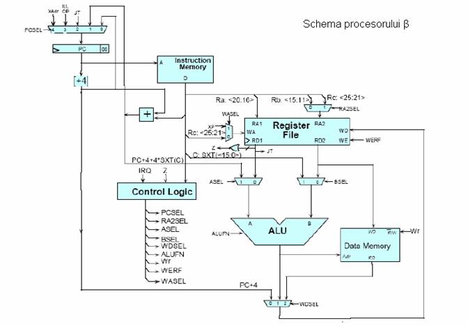
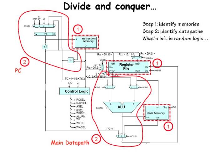
Prezentarea schemei procesorului si descrierea resurselor hardware la nivel de locuri structurale, cu indicarea semnalelor de intrare, iesire, comanda, sincronizare.
Prezentarea procesorului la nivelul Arhitecturii Setului de Instructiuni (coduri de operatii, moduri de adresare, conditii etc) .
Prezentarea modulelor Verilog pentru componentele structurale de la punctul 1.
Simularea sistemului in Verilog, plecand de la un program in cod masina scris pentru .
Completarea schemei cu interfetele pentru tastatura si monitor, in conformitate cu lucrarile de laborator efectuate anterior.
Experimentarea conectarii tastaturii si a monitorului: introducerea de programe de la tastatura si afisarea informatiilor relevante pe ecranul monitorului
Logica de comanda/control:
|
OP |
OPC |
LD |
ST |
JMP |
BEQ |
BNE |
LDR |
IllOP |
trap |
|
|
ALUFN |
F (op) |
F (op) |
"+" |
"+" |
- |
- |
- |
'A' |
- |
- |
|
WERF |
1 |
1 |
1 |
0 |
1 |
1 |
1 |
1 |
1 |
1 |
|
BSEL |
0 |
1 |
1 |
1 |
- |
- |
- |
- |
- |
- |
|
WDSEL |
1 |
1 |
2 |
- |
0 |
0 |
0 |
2 |
0 |
0 |
|
WR |
0 |
0 |
0 |
1 |
0 |
0 |
0 |
0 |
0 |
0 |
|
RA2SEL |
0 |
- |
- |
1 |
- |
- |
- |
- |
- |
- |
|
PCSEL |
0 |
0 |
0 |
0 |
2 |
Z ? 1 : 0 |
Z ? 0 : 1 |
0 |
3 |
4 |
|
ASEL |
0 |
0 |
0 |
0 |
- |
- |
- |
1 |
- |
- |
|
WASEL |
0 |
0 |
0 |
- |
0 |
0 |
0 |
0 |
1 |
1 |
Formatul instructiunilor
Operate Class:
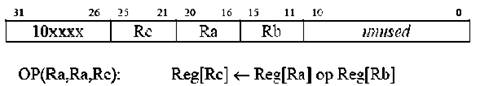
Coduri de operatii: ADD (plus) , SUB (minus) , MUL (multiply) , DIV (divided by)
AND (bitwise and) , OR (bitwise or) , XOR (bitwise exclusive or)
CMPEQ (equal) , CMFLT (less than) , CMPLE (less than or equal) [result = 1 if true, 0 if false], SHL (left shift) , SHR (light shift w/o sign extension) , SRA (right shift w/ sign extension)
|
Register |
Symbol |
Usage |
|
R31 |
R31 |
Always zero |
|
R30 |
XP |
Exception pointer |
|
R29 |
SP |
Stack pointer |
|
R28 |
LP |
Linkage pointer |
|
R27 |
BP |
Base of frame pointer |
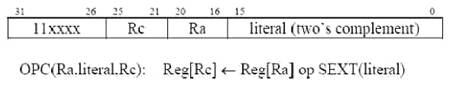
Coduri de opeartii: ADDC (plus) , SUBC (minus) , MULC (multiply) , DIVC (divided by) ANDC (bitwise and) . ORC bitwise or) , XORC (bitwise exclusive or)
CMFEQC (equal) , CMPLTC (less than) , CMPLEC (less than, or equal) [result = 1 if true, 0 if false] SHLC (left shift) , SHRC: (light shift w/o sign extension) , SRAC (right shift w) sign extension)
Other: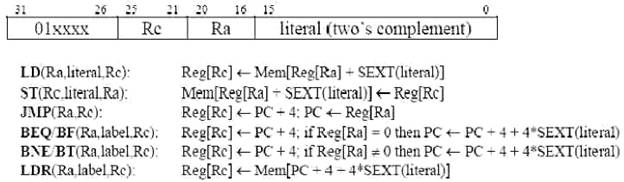
Tabelul codurilor de operatie: (coduri optionale de operatie)
|
2:0 S:3 | ||||||||
|
OOO | ||||||||
|
LD |
ST |
JMP |
BEQ |
BNE |
ldR |
|||
|
ADD |
SUB |
MUL* |
DIV* |
CMPEQ |
CMPLT |
CMPLEC | ||
|
AND |
OR |
XOR |
SHL |
SHR |
SRA | |||
|
ADDC |
SUBC |
MULC** |
DIVC* |
CMPEQC |
CMPLECC |
CMPLEC | ||
|
ANDC |
ORC |
XORC |
SHLC |
SRAC |
SRAC |
Ierarhia modulelor
. beta
control [random logic]
regfile [memory]
pc [datapath]
datapath
dp_ misc [datapath]
dp_ alu
dp_ addsub [datapath]
dp_ boote [datapath]
dp_ shift [datapath]
dp_ cmp [datapath]
dp_ mux [datapath]
. dp_ wdata [datapath]
Modulele Verilog pentru componentele structurale
// Beta PC logic
module pc (clk, reset, pcsel, offset, jump_ addr, branch_ addr, pc, pc_ plus_ 4) ; input clk;
input reset; // forces PC to 0x80000000
input [2:0] pcsel; // selects source of next PC
input [15:0] offset; // inst[15:0]
input
[31:0] jump_ addr; // from Reg[RA], used in JMP instruction
output [31:0] branch_ addr; //
send to datapath for LDR instruction
output [31:0] pc; // used as
address for instruction fetch
output [31:0] pc_ plus_ 4;// saved in regfile during branches, JMP, traps
reg [31:0] pc;
wire [30:0] pcinc;
wire [31:0] npc;
// the Beta PC increments by 4, but won't change supervisor bit
assign pcinc = pc + 4;
assign pc_ plus_ 4 = ;
// branch address = PC + 4 + 4*sxt (offset) assign branch_ addr = }, offset[15:0], 2'b00}};
assign npc = reset ? 32'h80000000 :
(pcsel = =0) ? : // normal
(pcsel = =) ? : // branch
(pcsel = =) ? : //jump
(pcsel = = 3) ? 32'h80000004 :
(pcsel = = 4) ? 32'h80000008 : // illop, trap
32'hXXXXXXXX; // catch errors
// pc register, pc[31] is supervisor bit and gets special treatment
always @ (posedge clk) pc <= npc;
endmodule
// 2-read, 1-write 32-location register file
module regfile (ra1, rd1, ra2, rd2, clk, werf, wa, wd) ;
input [4:0] ra1; // address for read port 1 (Reg[RA])
output [31:0] rd1; // read data for port 1
input [4:0] ra2; // address for read port 2 (Reg[RB], Reg[RC] for ST)
output [31:0] rd2; // read data for port 2
input clk;
input werf; // write enable, active high
input [4:0] wa; // address for write port (Reg[RC])
input [31:0] wd; // write data
reg [31:0] registers[31:0]; // the register file itself
// read paths are combinational
// logic to ensure R31 reads as zero is in main datapath
assign rd1 = registers[ra1];
assign rd2 = registers[ra2];
// write port is active only when WERF is asserted always @ (posedge clk)
if (werf) registers[wa] <= wd; endmodule
module dp_ addsub (fn, alu_ a, alu_ b, result, n, v, z) ;
input fn; // 0 for add, 1 for subtract
input [31:0] alu_ a; // A operand
input [31:0] alu_ b; // B operand
output [31:0] result; // result
output n, v, z; // condition codes computed from result
reg n, v, z;
reg [31:0] result;
always @ (fn or alu_ a or alu_ b) begin: ripple
integer i; // FOR loop index, not in hardware
reg cin, p, g; // expanded at compile time into many signals
reg [31:0] xb; // hold's complement of ALU_ B during subtract
// simple ripple-carry adder for now
xb = fn ? ~alu_ b : alu_ b; // a - b == a + ~b + 1
cin = fn; // carry in is 0 for add, 1 for sub
// remember: this FOR is expanded at *compile* time
for (i = 0; i < 32; i = i + 1) begin
p = alu_ a[i] ^ xb[i]; // carry propagate
g = alu_ a[i] & xb[i]; // carry generate
result[i] = p ^ cin;
cn = g | (p & cin) ; // carry into next stage
end
n = result[31]; // negative
z=~|result; // zero
v = (alu_ a[31] & xb[31] & !n) | (~alu_ a[31] & ~xb[31] & n) ;//overfl
end
endmodule
// fn == 2'b01: eq (Z)
// fn == 2'b10: lt (N ^ V)
// fn == 2'b11: le (Z | (N ^ V) )
// result is 1 if comparison is true, 0 otherwise
module dp_ cmp (fn, n, v, z, result) ;
input [1:0] fn;
input n, v, z;
output [31:0] result;
assign result = ;
endmodule
// fn == 2'b00: logical shift left
// fn == 2'b01: logical shift right
// fn == 2'b11: arithmetic shift right
module dp_ shift (fn, alu_ a, alu_ b, result) ;
input [1:0] fn;
input [31:0] alu_ a;
input [4:0] alu_ b;
output [31:0] result;
wire sin;
reg [31:0] u, result;
wire [31:0] v, w, x, y, z;
assign sin = fn[1] & alu_ a[31];
// assign u = fn[0] ? alu_ a[0:31] : alu_ a[31:0]
always @ (fn[0] or alu_ a) begin: loopA
integer i;
for (i = 0; i < 32; i = i + 1)
u[i] = fn[0] ? alu_ a[31 - i] : alu_ a[i];
end
assign v = alu_ b[4] ? }} : u[31:0];
assign w = alu_ b[3] ? }} : v[31:0];
assign x = alu_ b[2] ? }} : w[31:0];
assign y = alu_ b[1] ? }} : x[31:0];
assign z = alu_ b[0] ? : y[31:0];
// assign result = fn[0] ? z[0:31] : z[31:0]
always @ (fn[0] or z) begin: loopB
integer i;
for (i = 0; i < 32; i = i + 1)
result[i] = fn[0] ? z[31 - i] : z[i];
end
endmodule
// fn is truth table for boolean operation:
// AND: fn = 4'b1000
// OR: fn = 4'b1110
// XOR: fn = 4'b0110
// A: fn = 4'b1010
module dp_ boole (fn, alu_ a, alu_ b, result) ;
input [3:0] fn;
input [31:0] alu_ a, alu_ b;
output [31:0] result;
reg [31:0] result;
always @ (fn or alu_ a or alu_ b) begin: bits integer i; for (i = 0; i < 32; i = i + 1) begin
result[i] = alu_ b[i] ? (alu_ a[i] ? fn[3] : fn[2]) :
(alu_ a[i] ? fn[1] : fn[0]) ;
end
end
endmodule
module dp_ mux (sel, addsub, boole, shift, cmp, alu) ;
input [1:0] sel;
input [31:0] addsub;
input [31:0] boole;
input [31:0] shift;
input [31:0] cmp;
output [31:0] alu;
assign alu = (sel == 2'b00) ? addsub :
(sel == 2'b01) ? boole :
(sel == 2'b10) ? shift :
(sel == 2'b11) ? cmp :
32'hXXXXXXXX;
endmodule
module dp_ misc (rd1zero, rd2zero, asel, bsel, inst, rd1, rd2, branch_ addr,
alu_ a, alu_ b, jump_ addr, mem_ wr_ data, z) ;
input
rd1zero; //
RA == R31, so treat RD1 as 0
input rd2zero; // RB/RC == R31, so treat RD2 as 0
input asel; // select A operand for ALU
input bsel; // select B operand for ALU
input
[15:0] inst; // constant field from
instruction
input [31:0] rd1; // Reg[RA] from
register file
input [31:0] rd2; // Reg[RB] from register file (Reg[RC] for ST)
input [31:0] branch_ addr; // PC + 4 + 4*sxt (inst[15:0])
output [31:0] alu_ a; // A input to ALU
output [31:0] alu_ b; // B input to ALU
output [31:0] jump_ addr; // jump address (from Reg[RA])
output [31:0] mem_ wr_ data; // data memory write data
output z; // true if Reg[RA] is zero, used during branches
// R31 reads as 0, so make that adjustment here
assign jump_ addr = rd1zero ? 32'b0 : rd1;
assign mem_ wr_ data = rd2zero ? 32'b0 : rd2;
assign z = ~|jump_ addr;
assign alu_ a = asel ? branch_ addr : jump_ addr;
assign alu_ b = bsel[0] ? }, inst[15:0]} : mem_ wr_ data;
endmodule
module dp_ alu (alufn, alu_ a, alu_ b, alu) ; input [5:0] alufn; input [31:0] alu_ a; input [31:0] alu_ b; output [31:0] alu;
wire [31:0] addsub;
wire [31:0] boole;
wire [31:0] shift;
wire [31:0] cmp;
wire alu_ n;
wire alu_ v;
wire alu_ z;
// the four functional units
dp_ addsub alu1 (alufn[0], alu_ a, alu_ b, addsub, alu_ n, alu_ v, alu_ z) ;
dp_ boole alu4 (alufn[3:0], alu_ a, alu_ b, boole) ;
dp_ shift alu3 (alufn[1:0], alu_ a, alu_ b[4:0], shift) ;
dp_ cmp alu2 (alufn[2:1], alu_ n, alu_ v, alu_ z, cmp) ;
// 4-to-1 mux selects alu output from functional units
dp_ mux alu5 (alufn[5:4], addsub, boole, shift, cmp, alu) ;
endmodule
module dp_ wdata (wdsel, pc_ plus_ 4, alu, mem_ data, wdata) ;
input [1:0] wdsel;
nput [31:0] pc_ plus_ 4;
input [31:0] alu;
input [31:0] mem_ data;
output [31:0] wdata;
assign wdata = wdsel[1] ? mem_ data :
wdsel[0] ? alu : pc_ plus_ 4; endmodule
module
datapath (inst, rd1, rd2, pc_ plus_ 4, branch_ addr, mem_ rd_ data,
rd1zero, rd2zero, asel, bsel, wdsel, alufn,
wdata, mem_ addr, jump_ addr, mem_ wr_ data, z) ;
input [15:0] inst; // constant
field from instruction
input [31:0] rd1; // Reg[RA] from
register file
input
[31:0] rd2; // Reg[RB] from register
file (Reg[RC] for ST)
input [31:0] pc_ plus_ 4; //
incremented PC
input [31:0] branch_ addr; // PC + 4 + 4*sxt (inst[15:0])
input [31:0] mem_ rd_ data; // memory read data (for LD)
input rd1zero; // RA == R31, so treat RD1 as 0
input rd2zero; // RB/RC == R31, so treat RD2 as 0
input asel; // select A operand for ALU
input bsel; // select B operand for ALU
input [1:0] wdsel; // select regfile write data
input [5:0] alufn; // operation to
be performed by alu
output [31:0] wdata; // regfile write data (output of WDSEL
mux)
output [31:0] mem_ addr; // alu output, doubles as data memory address
output [31:0] jump_ addr; // jump
address (from Reg[RA])
output [31:0] mem_ wr_ data; // data
memory write data (from Reg[RC])
output z; //
true if Reg[RA] is zero, used during branches
wire [31:0] alu_ a; // A input to ALU
wire [31:0] alu_ b; // B input to ALU
// compute A and B inputs into alu, also Z bit for control logic
dp_ misc misc (rd1zero, rd2zero, asel, bsel, inst, rd1, rd2, branch_ addr,
alu_ a, alu_ b, jump_ addr, mem_ wr_ data, z) ;
// where all the heavy-lifting happens
dp_ alu alu (alufn, alu_ a, alu_ b, mem_ addr) ;
// select regfile write data from PC+4, alu output, and memory data
dp_ wdata wdata (wdsel, pc_ plus_ 4, mem_ addr, mem_ rd_ data, wdata) ;
endmodule
module control (reset, irq, supervisor, z, inst,
alufn, asel, bsel, pcsel, ra2, rd1zero, rd2zero, wa, wdsel, werf, mem_ we) ;
input reset; // active high
input irq; // interrupt request, active high
input supervisor; // 1 for kernel-mode, 0 for user-mode
input z; // Reg[RA] == 0, used for branch tests
input [31:0] inst; // current instruction
output [5:0] alufn; // selects ALU function
output asel; // selects ALU A operand
output bsel; // selects ALU B operand
output [2:0] pcsel; // selects next PC
output [4:0] ra2; // RB or RC
output rd1zero; // RA == 31
output rd2zero; // ra2 == 31
output [4:0] wa; // RC or XP
output [1:0] wdsel; // selects regfile write data
output werf; // regfile write enable
output mem_ we; // memory write enable, active high
reg [15:0] ctl; // local
wire interrupt;
// interrupts enabled in user mode only
assign interrupt = irq & ~supervisor;
// control ROM
always @ (inst or interrupt) begin if (interrupt)
ctl = 16'bx_ 100_ 1xx_ xxxxxx_ 00_ 0; //
interrupt
else case (inst[31:26])
ppp aaaaaa ww
b ccc w llllll dd
t sss aab uuuuuu ss
e eee sss ffffff ee x
s lll eee nnnnnn ll w
t 210 lll 543210 10 r
default: ctl = 16'bx_ 011_ 1xx_ xxxxxx_ 00_ 0; // illegal opcod
6'b011000: ctl = 16'bx_ 000_ 001_ 00xxx0_ 10_ 0; // LD
6'b011001: ctl = 16'bx_ 000_ x01_ 00xxx0_ 10_ 1; // ST
6'b011011: ctl = 16'bx_ 010_ 0xx_ xxxxxx_ 00_ 0; // JMP
6'b011101: ctl = 16'b1_ 001_ 0xx_ xxxxxx_ 00_ 0; // BEQ
6'b011110: ctl = 16'b0_ 001_ 0xx_ xxxxxx_ 00_ 0; // BNE
6'b011111: ctl = 16'bx_ 000_ 010_ 011010_ 10_ 0; // LDR
6'b100000: ctl = 16'bx_ 000_ 000_ 00xxx0_ 01_ 0; // ADD
6'b100001: ctl = 16'bx_ 000_ 000_ 00xxx1_ 01_ 0; // SUB
6'b100100: ctl = 16'bx_ 000_ 000_ 11x011_ 01_ 0; // CMPEQ
6'b100101: ctl = 16'bx_ 000_ 000_ 11x101_ 01_ 0; // CMPLT
6'b100110: ctl = 16'bx_ 000_ 000_ 11x111_ 01_ 0; // CMPLE
6'b101000: ctl = 16'bx_ 000_ 000_ 011000_ 01_ 0; // AND
6'b101001: ctl = 16'bx_ 000_ 000_ 011110_ 01_ 0; // OR
6'b101010: ctl = 16'bx_ 000_ 000_ 010110_ 01_ 0; // XOR
6'b101100: ctl = 16'bx_ 000_ 000_ 10xx00_ 01_ 0; // SHL
6'b101101: ctl = 16'bx_ 000_ 000_ 10xx01_ 01_ 0; // SHR
6'b101110: ctl = 16'bx_ 000_ 000_ 10xx11_ 01_ 0; // SRA
6'b110000: ctl = 16'bx_ 000_ 001_ 00xxx0_ 01_ 0; // ADDC
6'b110001: ctl = 16'bx_ 000_ 001_ 00xxx1_ 01_ 0; // SUBC
6'b110100: ctl = 16'bx_ 000_ 001_ 11x011_ 01_ 0; // CMPEQC
6'b110101: ctl = 16'bx_ 000_ 001_ 11x101_ 01_ 0; // CMPLTC
6'b110110: ctl = 16'bx_ 000_ 001_ 11x111_ 01_ 0; // CMPLEC
6'b111000: ctl = 16'bx_ 000_ 001_ 011000_ 01_ 0; // ANDC
6'b111001: ctl = 16'bx_ 000_ 001_ 011110_ 01_ 0; // ORC
6'b111010: ctl = 16'bx_ 000_ 001_ 010110_ 01_ 0; // XORC
6'b111100: ctl = 16'bx_ 000_ 001_ 10xx00_ 01_ 0; // SHLC
6'b111101: ctl = 16'bx_ 000_ 001_ 10xx01_ 01_ 0; // SHRC
6'b111110: ctl = 16'bx_ 000_ 001_ 10xx11_ 01_ 0; //
SRAC
endcase
end
assign werf = ~ctl[0];
assign mem_ we = !reset & ctl[0];
assign wdsel = ctl[2:1];
assign alufn = ctl[8:3];
assign bsel = ctl[9];
assign asel = ctl[10];
assign wa = ctl[11] ? 5'b11110 : inst[25:21];
assign pcsel = ( (ctl[14:12] == 3'b001) & (ctl[15] ^ z) ) ? 3'b000 : ctl[14:12];
assign ra2 = ctl[0] ? inst[25:21] : inst[15:11];
assign rd1zero = (inst[20:16] == 5'b11111) ;
assign rd2zero = (ra2 == 5'b11111) ;
endmodule
module beta (clk, reset, irq, inst_ addr, inst_ data,
mem_ addr, mem_ rd_ data, mem_ we, mem_ wr_ data) ; input clk;
input reset; // active high
input irq; // interrupt request, active high
output
[31:0] inst_ addr; // address of
instruction to be fetched
input [31:0] inst_ data; //
instruction returning from memory
output [31:0] mem_ addr; // address
of data word to be accessed
input [31:0] mem_ rd_ data; // read data
returning from memory
output mem_ we; // memory write enable, active
high
output [31:0] mem_ wr_ data; // memory write data
// internal signals source description
wire [5:0] alufn; // [control] selects ALU function
wire asel; // [control] selects ALU A operand
wire [31:0] branch_ addr; // [pc] PC + 4 +4*sxt (inst[15:0])
wire bsel;
// [control] selects ALU B operand
wire [31:0] jump_ addr; // [datapath] Reg[RA]
wire [31:0] pc_ plus_ 4; // [pc] PC + 4
wire [2:0] pcsel; // [control] selects next PC
wire [4:0] ra2; // [control] RB or RC
wire [31:0] rd1; // [regfile] Reg[RA]
wire rd1zero; // [control] RA == 31
wire [31:0] rd2; // [regfile] Reg[ra2]
wire rd2zero; // [control] ra2 == 31
wire [4:0] wa; // [control] RC or XP
wire [1:0] wdsel; // [control] selects regfile write data
wire werf; // [control] regfile write enable
wire [31:0] wdata; // [datapath] regfile write data
wire z; // [datapath] Reg[RA] == 0
// control logic, reg file address generation
control ctl (reset, irq, inst_ addr[31], z, inst_ data[31:0],
alufn, asel, bsel, pcsel, ra2, rd1zero, rd2zero, wa, wdsel, werf, mem_ we) ;
// program counter logic
pc pc (clk, reset, pcsel, inst_ data[15:0], jump_ addr, branch_ addr, inst_ addr, pc_ plus_ 4) ;
// register file
regfile regfile (inst_ data[20:16], rd1, ra2, rd2, clk, werf, wa, wdata) ;
// datapath datapath dp (inst_ data[15:0], rd1, rd2, pc_ plus_ 4, branch_ addr, mem_ rd_ data,
rd1zero, rd2zero, asel, bsel, wdsel, alufn, wdata, mem_ addr, jump_ addr, mem_ wr_ data, z) ; endmodule
//Modulul principal main (top.v)
// Set time units to be nanoseconds.
`timescale 1ns / 1ps
module VGATestTop (clk, clr, store, sw, ps_ data, ps_ clk, hsync, vsync, r2, r1, r0, g2, g1, g0, b2, b1, b0, led, cled) ;
input clk;
input clr;
input store;
input sw;
inout ps_ data;
inout ps_ clk;
output hsync;
output vsync;
output r2, r1, r0, g2, g1, g0, b2, b1, b0;
output [7:0] led;
output cled;
reg r2, r1, r0, g2, g1, g0, b2, b1, b0;
wire active;
wire [11:0] x;
wire [11:0] y;
wire [7:0] led;
wire cled;
reg [25:0] cnt;
wire [0:31] display_ word;
wire [31:0] douti;
wire [7:0] addri;
wire [0:3] display_ byte, display;
wire [2:0] dtx, dty;
wire [2:0] tmp;
reg bclk, reset, irq=1'b0;
wire [31:0] inst_ addr;
wire [31:0] inst_ data;
wire [31:0] mem_ addr;
wire [31:0] mem_ wr_ data;
wire [31:0] mem_ rd_ data;
wire mem_ we;
wire [8:0] video_ rd_ addr;
wire [31:0] video_ rd_ data;
wire [8:0] addrc;
wire [0:7] doutc;
wire bord, mem_ display, ps_ display, current_ instr, current_ data, ind;
wire new_ scancode, new_ data;
wire [4:0] dsb0, dsb1, dsb2, dsb3;
wire [7:0] scancode;
wire [3:0] data_ from_ ps2;
reg [3:0] ps_ instr [9:0];
reg [3:0] ps_ pointer;
reg [3:0] char_ pointer;
reg saved;
reg wea, instr_ clk;
reg [7:0] addra;
reg [31:0] dina;
reg rx_ read;
wire rx_ extended, rx_ released, rx_ shift_ key_ on, tx_ write_ ack_ o, tx_ error_ no_ keyboard_ ack;
wire [7:0] rx_ ascii;
VGATimer # (800, 64, 120, 56, 600, 23, 6, 37, 1) timer (clk, hsync, vsync, active, x, y) ;
char_ rom char (addrc, ~clk, doutc) ;
data_ ram video_ data (mem_ addr[10:2], video_ rd_ addr, bclk, ~clk, mem_ wr_ data, video_ rd_ data, mem_ we) ;
scancod2cod code (scancode, rx_ released, data_ from_ ps2, new_ data) ;
ps2_ keyboard_ interface ps2 (clk, ~clr, ps_ clk, ps_ data, rx_ extended, rx_ released, rx_ shift_ key_ on, scancode, rx_ ascii, new_ scancode, rx_ read, 8'd0, 1'b0, tx_ write_ ack_ o, tx_ error_ no_ keyboard_ ack) ;
inst_ rom inst (addra, addri, instr_ clk, ~clk, dina, inst_ data, douti, wea) ;
data_ ram data (mem_ addr[10:2], mem_ addr[10:2], bclk, bclk, mem_ wr_ data, mem_ rd_ data, mem_ we) ;
beta beta (bclk, reset, irq, inst_ addr, inst_ data, mem_ addr, mem_ rd_ data, mem_ we, mem_ wr_ data) ;
always @ (posedge clk)
rx_ read <= (new_ data) ? saved: ~saved;
always @ (negedge clr or posedge bclk)
if (~clr) reset <= 1;
else reset <= 0;
always @ (negedge clr or posedge clk)
if (~clr) cnt <= 0;
else cnt <= cnt+1;
always @ (negedge clr or posedge clk)
if (~clr) bclk <= 0;
else if (sw) bclk <= cnt[25];
else bclk <= 0;
always @ (posedge clk)
if (new_ data) begin
if (~saved) begin
saved <= 1;
ps_ instr[ps_ pointer] <= data_ from_ ps2;
if (ps_ pointer<9) ps_ pointer <= ps_ pointer+1;
else ps_ pointer <= 0;
end
end else saved <= 0;
always @ (posedge clk)
if (store&~sw) begin
dina <= ;
addra <= ;
wea <= 1;
instr_ clk <= cnt[25];
end else begin
addra <= inst_ addr[9:2];
wea <= 0;
instr_ clk <= cnt[25];
end
assign addrc = ;
assign addri=;
assign tmp= (x[9:8]==2'b10) ? 1'b1 : 1'b0;
assign video_ rd_ addr=;
assign ind = (x<256) ;
assign display_ word= (ind) ? douti:video_ rd_ data;
assign dsb0=;
assign dsb1=;
assign dsb2=;
assign dsb3=;
assign display_ byte=;
assign display= (y[9]) ? ps_ instr[char_ pointer]:display_ byte;
assign dtx=x[2:0];
assign dty=y[2:0];
assign bord= ( (x==0) | (x==799) | (x[5:0]==6'b000000) & (y<512) | (y==0) | (y==599) | (y==511) ) ;
assign mem_ display= (y<=511) & (x<767) ;
assign ps_ display= (y[9]) & (ind) & (y[5:3]==3'b101) & ( (x[8:3]>10) & (x[8:3]<13) | (x[8:3]>15) & (x[8:3]<24) ) ;
assign current_ instr= (addri==inst_ addr[9:2]) & (ind) ;
assign current_ data= (video_ rd_ addr==mem_ addr[10:2]) & (~ind) ;
assign cled=cnt[25];//new_ data;
always @ (posedge clk)
begin
case (x[8:3])
6'd11 : char_ pointer <= 4'd0;
6'd12 : char_ pointer <= 4'd1;
6'd16 : char_ pointer <= 4'd2;
6'd17 : char_ pointer <= 4'd3;
6'd18 : char_ pointer <= 4'd4;
6'd19 : char_ pointer <= 4'd5;
6'd20 : char_ pointer <= 4'd6;
6'd21 : char_ pointer <= 4'd7;
6'd22 : char_ pointer <= 4'd8;
6'd23 : char_ pointer <= 4'd9;
default : char_ pointer <= 4'd0;
endcase
r2 <= active&& ( (ps_ display&&doutc[dtx]&& (ps_ pointer>char_ pointer) ) || (mem_ display&&doutc[dtx]&&~current_ data) ) ;
r1 <= active&& ( (ps_ display&&doutc[dtx]) || (mem_ display&&doutc[dtx]&&ind&&~current_ data) ) ;
r0 <= active&& ( (ps_ display&&doutc[dtx]) || (mem_ display&&doutc[dtx]&& (x[6]^^ind) &&~current_ data) ) ;
g2 <= active&& ( (ps_ display&&doutc[dtx]&& (ps_ pointer>char_ pointer) ) || (mem_ display&&doutc[dtx]&&~current_ instr) ) ;
g1 <= active&& ( (ps_ display&&doutc[dtx]) || (mem_ display&&doutc[dtx]&&ind&&~current_ instr) ) ;
g0 <= active&& ( (ps_ display&&doutc[dtx]) || (mem_ display&&doutc[dtx]&& (x[6]^^ind) &&~current_ instr) ) ;
b2 <= active&& ( (ps_ display&&doutc[dtx]&& (ps_ pointer>char_ pointer) ) || (mem_ display&&doutc[dtx]&&~current_ instr&&~current_ data) ||bord) ;
b1 <= active&& ( (ps_ display&&doutc[dtx]) || (mem_ display&&doutc[dtx]&&ind&&~current_ instr&&~current_ data) ||bord) ;
b0 <= active&& ( (ps_ display&&doutc[dtx]) || (mem_ display&&doutc[dtx]&& (x[6]^^ind) &&~current_ instr&&~current_ data) ||bord) ;
end
assign led = scancode;
endmodule
|
